

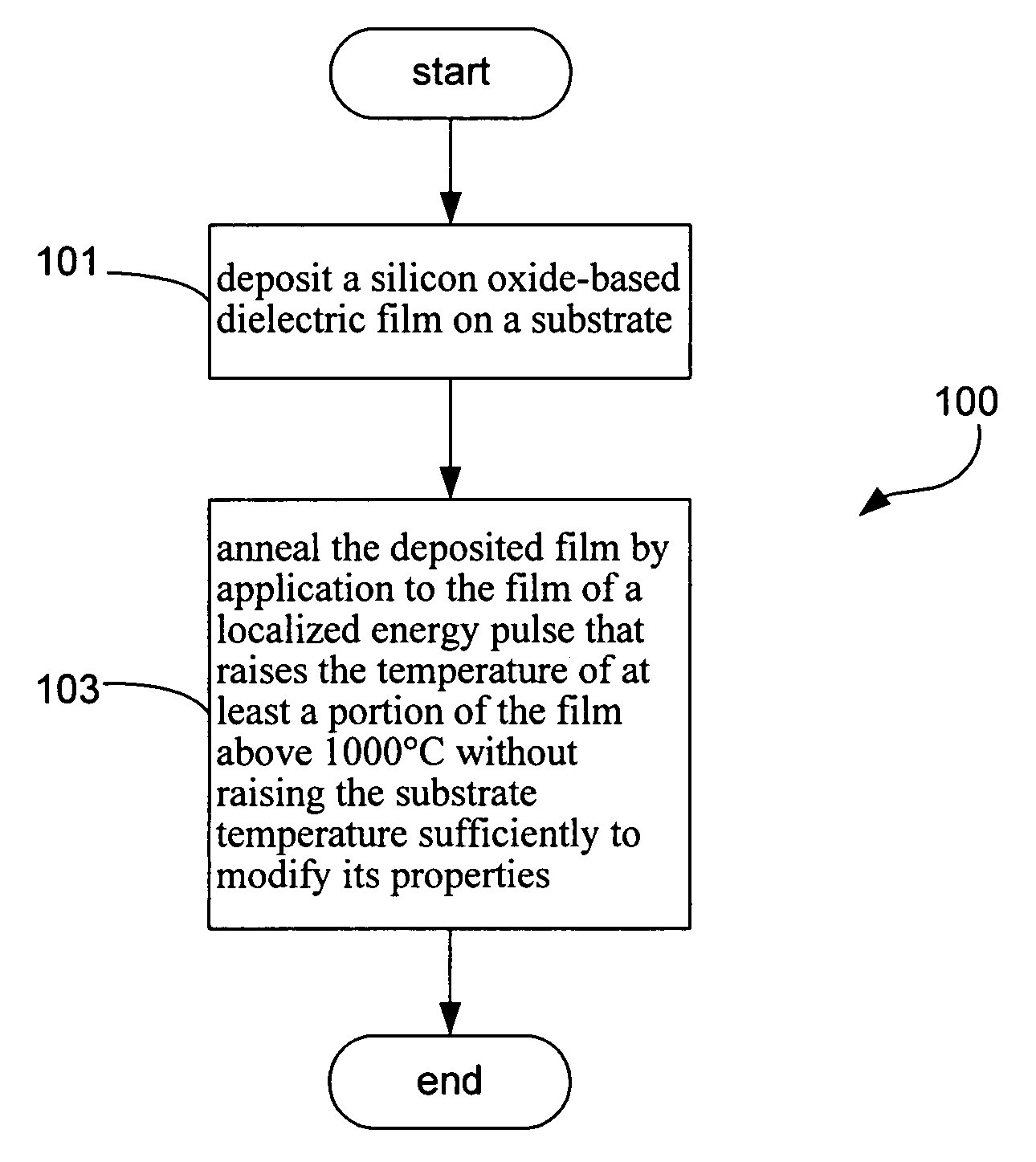
Localized energy pulse rapid thermal anneal dielectric film densification method
a dielectric film and local energy pulse technology, applied in the direction of basic electric elements, electric apparatus, semiconductor/solid-state device manufacturing, etc., can solve the problems of reducing budgets, increasing difficulty in void-free filling of high aspect ratio spaces (ar>3.0:1), and shrinking dimensions
- Summary
- Abstract
- Description
- Claims
- Application Information
AI Technical Summary
Benefits of technology
Problems solved by technology
Method used
Image

Examples
example
[0064]The following example provides details relating to performance advantages of the present invention. It should be understood the following is representative only, and that the invention is not limited by the detail set forth in this example.
[0065]Referring to FIGS. 5A–B, STI trenches 502 in a Si-based semiconductor substrate 500 were filled by depositing a silicon-oxide film 504 with a PDL process using trimethylaluminum (Al(CH3)3) as a metal catalyst-containing precursor and tris(tert-pentoxy)silanol ((C5H11O)3SiOH) as the silicon containing precursor. Following completion of the deposition, a seam 506 remained between opposing faces of the dielectric film 504 deposited in the trenches 502, as illustrated in FIG. 5A which shows a sample trench post-deposition but pre-annealing. Annealing was conducted by a laser pulse annealing technique in accordance with the present invention in which an excimer laser operating at a wavelength of about 193 nm was pulsed on the film 504 in ea...
PUM
| Property | Measurement | Unit |
|---|---|---|
| temperature | aaaaa | aaaaa |
| temperature | aaaaa | aaaaa |
| temperature | aaaaa | aaaaa |
Abstract
Description
Claims
Application Information