

Electro-optical device, method of manufacturing the same, and electronic apparatus
- Summary
- Abstract
- Description
- Claims
- Application Information
AI Technical Summary
Benefits of technology
Problems solved by technology
Method used
Image

Examples
Embodiment Construction
[0089]Hereinafter, an exemplary embodiment of the present invention is described below with reference to the attached drawings. According to the exemplary embodiment, an electro-optical device according to the present invention is applied to liquid crystal devices.
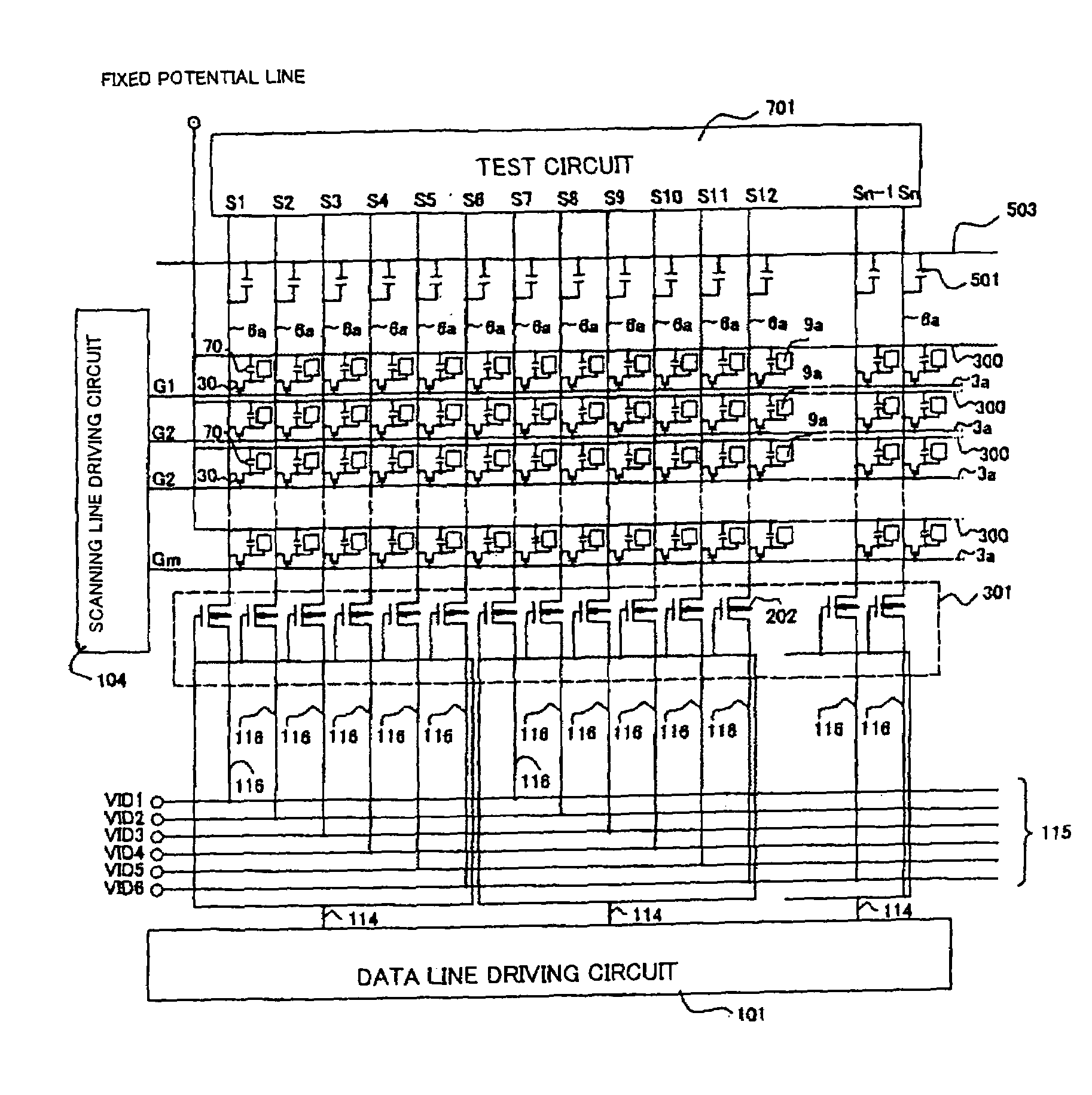
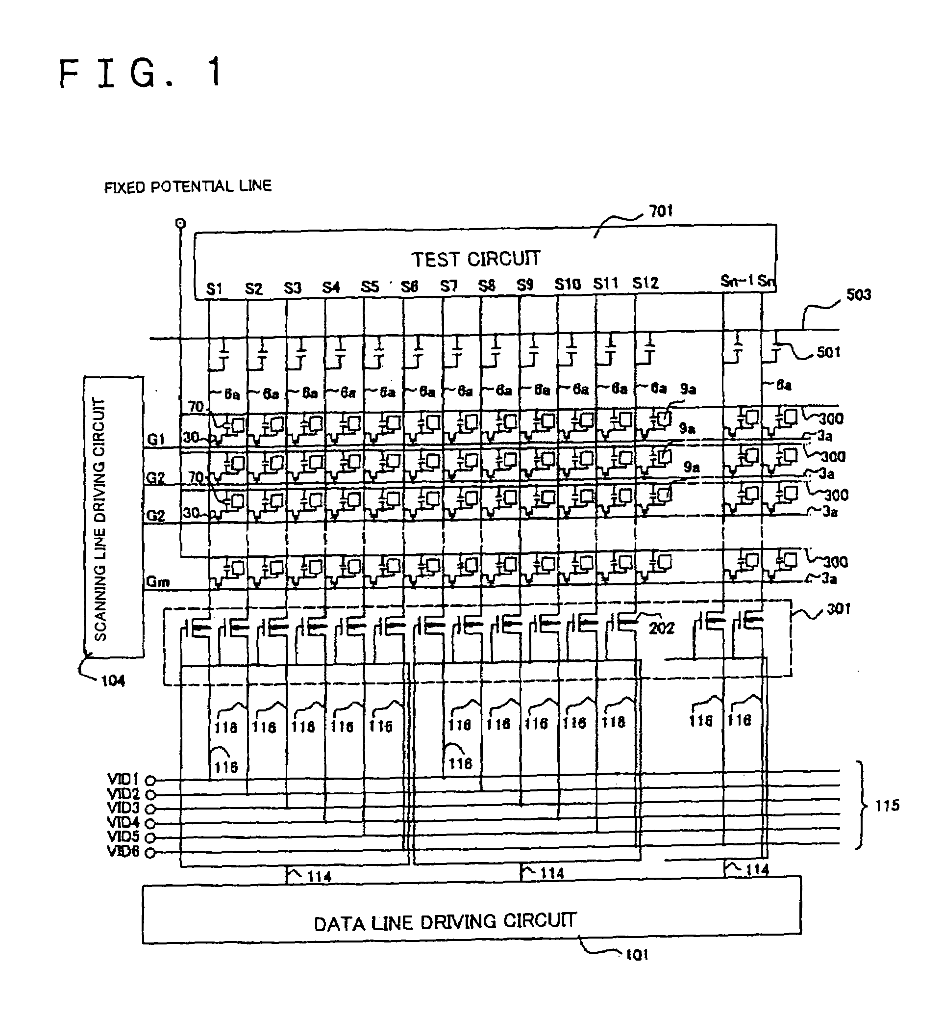
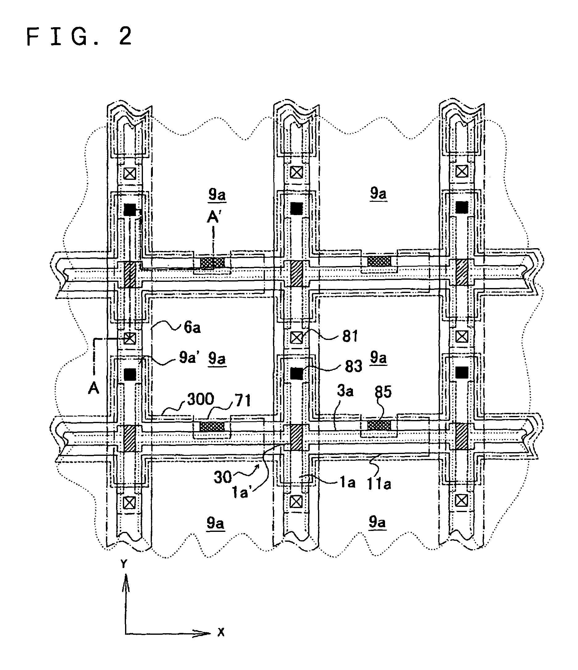
[0090]The structure of a pixel portion of an electro-optical device according to the exemplary embodiment of the present invention is described below with reference to FIGS. 1 to 3. FIG. 1 illustrates an equivalent circuit of various elements and wiring lines provided in a plurality of pixels which are arranged in a matrix and form an image display region of the electro-optical device. FIG. 2 is a plan view of a plurality of pixel groups adjacent to each other on the TFT array substrate, in which the data lines, the scanning lines, and the pixel electrodes are formed. FIG. 3 is a sectional view taken along the plane A–A′ of FIG. 2. In FIG. 3, respective layers and members are shown in different scales to make them recogniz...
PUM
 Abstract
Description
Claims
Application Information