Multi-level nonvolatile semiconductor memory device utilizing a nonvolatile semiconductor memory device for storing binary data

a nonvolatile semiconductor and memory device technology, applied in the field of semiconductor memory devices, can solve the problems of not taking into account the configuration for stably generating the basis voltage for the comparison, the difficulty of coexisting slc configuration and mlc configurations that are different in number of addresses, and the long period of time required for data read-out, etc., to achieve high speed

Active Publication Date: 2007-01-16
RENESAS ELECTRONICS CORP
View PDF11 Cites 78 Cited by
  • Summary
  • Abstract
  • Description
  • Claims
  • Application Information

AI Technical Summary

Benefits of technology

[0020]An object of the present invention is to provide a nonvolatile semiconductor memory device of an MLC configuration, compatible with an SLC configuration, for allowing writing and reading of multi-level data at high speed.
[0021]Another object of the present invention is to provide a nonvolatile semiconductor memory device of an MLC configuration allowing stable data read out in a page mode according to a serial sense scheme.
[0028]The first bit and the second bit of an address signal are switched in the second operation mode and thereby an increase in the address signal bit in the case when the SLC configuration is utilized for the MLC configuration can be easily accommodated without changing the internal configuration. In addition, a block address bit is utilized so that data in successive addresses can be stored in each block even in the MLC configuration.
[0029]Currents that flow through a plurality of reference cells are averaged and a reference voltage is generated in accordance with the averaged currents. Thus, a reference voltage at a desired voltage level can be stably generated without being affected by variation of the characteristics of the reference cells.
[0031]A sense amplifier circuit is arranged corresponding to each memory block and the data from the sense amplifier circuit is transferred to the first and second latch circuits for the same address. Thus, read out of data can be performed in the serial sense scheme even in storage of multi-bit data, and in addition, data read out in a page mode can be easily implemented.
[0032]When memory cell data is detected in the serial sense scheme, second time reference current is set in accordance with first time sensed data and thereby, data can be precisely sensed by the sense amplifier circuit for each word bit without changing the word line voltage.

Problems solved by technology

In such a case, one memory cell stores data bits of different addresses to make the allocations of addresses complicated and therefore, it becomes difficult to coexist an SLC configuration and an MLC configuration that are different in number of address bits
In data read out the word line voltage is changed and a problem arises that a long period of time is required for data read-out.
However, the configuration for stably generating the basis voltage for the comparison is not taken into consideration.
In addition, a sense amplifier for reading out 4-level data and a sense amplifier for reading out 2-level data are separately provided in the configuration shown in this Document 6 and therefore, the circuit configuration is redundant and a problem of increased circuit layout area arises.

Method used


Image

  • Multi-level nonvolatile semiconductor memory device utilizing a nonvolatile semiconductor memory device for storing binary data
  • Multi-level nonvolatile semiconductor memory device utilizing a nonvolatile semiconductor memory device for storing binary data
  • Multi-level nonvolatile semiconductor memory device utilizing a nonvolatile semiconductor memory device for storing binary data

Examples


first embodiment

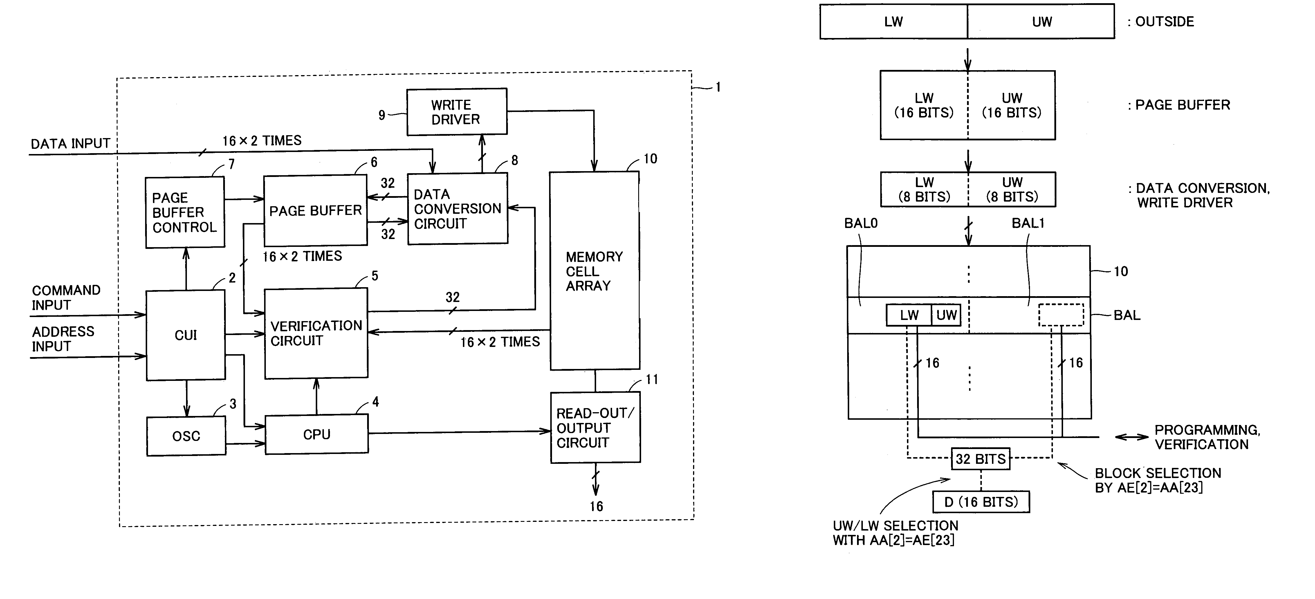
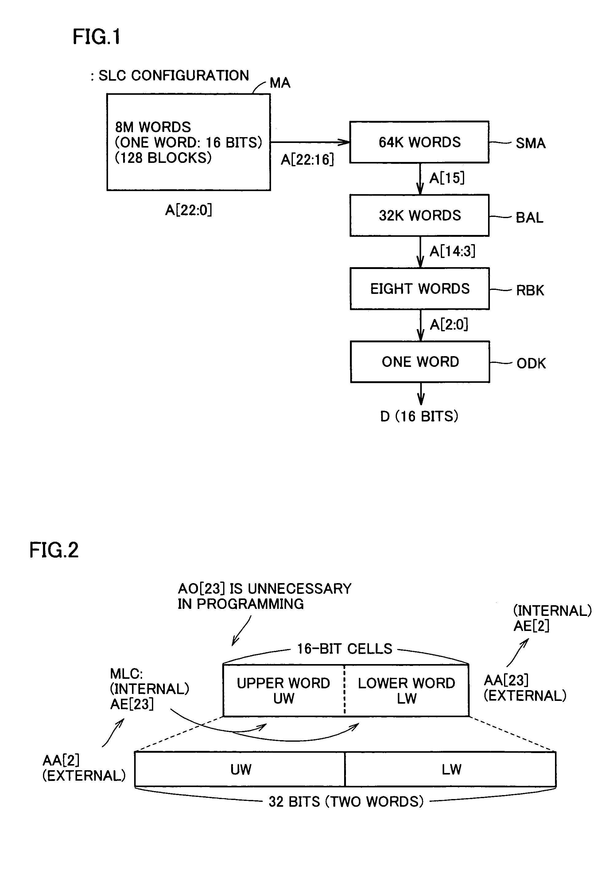
[0097]FIG. 1 is a diagram schematically showing the configuration of a memory array and the configuration of an address of a memory cell of a semiconductor memory device to which the present invention is applied. In FIG. 1, a memory array MA has memory cells of 8M words×16 bits. Here, 1 word is formed of 16 bits.

[0098]In memory array MA, 128 blocks of 64K words are provided. Accordingly, an address A [22:0] of 23 bits is used for selecting 1 word from these 8M words. Memory array MA is typically divided into two memory mats. Address bits A [22:16] are used for selecting a block SMA of 64K words. 64K word block SMA includes two 32K word blocks BAL. The 32K word block BAL is typically used as a sector and utilized as an erasure unit of data.

[0099]A read out data block RBK of 8 words is selected from 32K word block BAL in data reading out. Address bits A [14:3] are utilized for selecting the 8 words from 32K word block BAL. Address bits A [2:0] are utilized for finally selecting a read...


PUM


Abstract

A multi-level semiconductor memory device for storing multi-level data having three or more values is implemented by utilizing a nonvolatile memory device for storing 2-valued data. Identification of successive 16-bit data externally applied is performed with external address bit AA [2], and a storage block is selected with external address bit AA [23]. Upper word data LW and lower word data UW are compressed into byte data of 8 bits, respectively, and stored in a memory cell array.

Description

BACKGROUND OF THE INVENTION[0001]1. Field of the Invention[0002]The present invention relates to a semiconductor memory device and, in particular, relates to a nonvolatile semiconductor memory device that can store multi-level data having three or more levels in a nonvolatile manner. More specifically, the present invention relates to a configuration for implementing a multi-level nonvolatile semiconductor memory device that stores multi-level data by utilizing an internal configuration of a nonvolatile semiconductor memory device for storing binary data.[0003]2. Description of the Background Art[0004]In a nonvolatile semiconductor memory device for storing data in a nonvolatile manner, a memory cell is formed of a single transistor. Such a memory cell transistor has a floating gate that is formed between a control gate and a substrate region. This floating gate is electrically isolated from its surrounding and the threshold voltage of the memory cell transistor is determined depend...

Claims


Application Information

Patent Timeline
Patent Type & Authority Patents(United States)
IPC IPC(8): G11C16/00G11C16/08G11C11/56G11C16/02G11C16/04G11C16/06
CPCG11C11/56G11C8/10G11C7/1006G11C2211/5641G11C16/04G11C16/02G11C16/08
Inventor MITANI, HIDENORIYAMAUCHI, TADAAKIOGURA, TAKU
Owner RENESAS ELECTRONICS CORP
Why Eureka
Try Eureka