NVRAM memory cell architecture that integrates conventional SRAM and flash cells

a memory cell and flash cell technology, applied in static storage, digital storage, instruments, etc., can solve the problems of data loss, volatile data retained in the memory cell,

Inactive Publication Date: 2007-01-16
ABEDNEJA ASSETAB L L C
View PDF7 Cites 273 Cited by
  • Summary
  • Abstract
  • Description
  • Claims
  • Application Information

AI Technical Summary

Problems solved by technology

The data retained in the memory cell is volatile, in that any interruption of the power supply voltage source causes a loss of the data.

Method used


Image

  • NVRAM memory cell architecture that integrates conventional SRAM and flash cells
  • NVRAM memory cell architecture that integrates conventional SRAM and flash cells
  • NVRAM memory cell architecture that integrates conventional SRAM and flash cells

Examples


Embodiment Construction

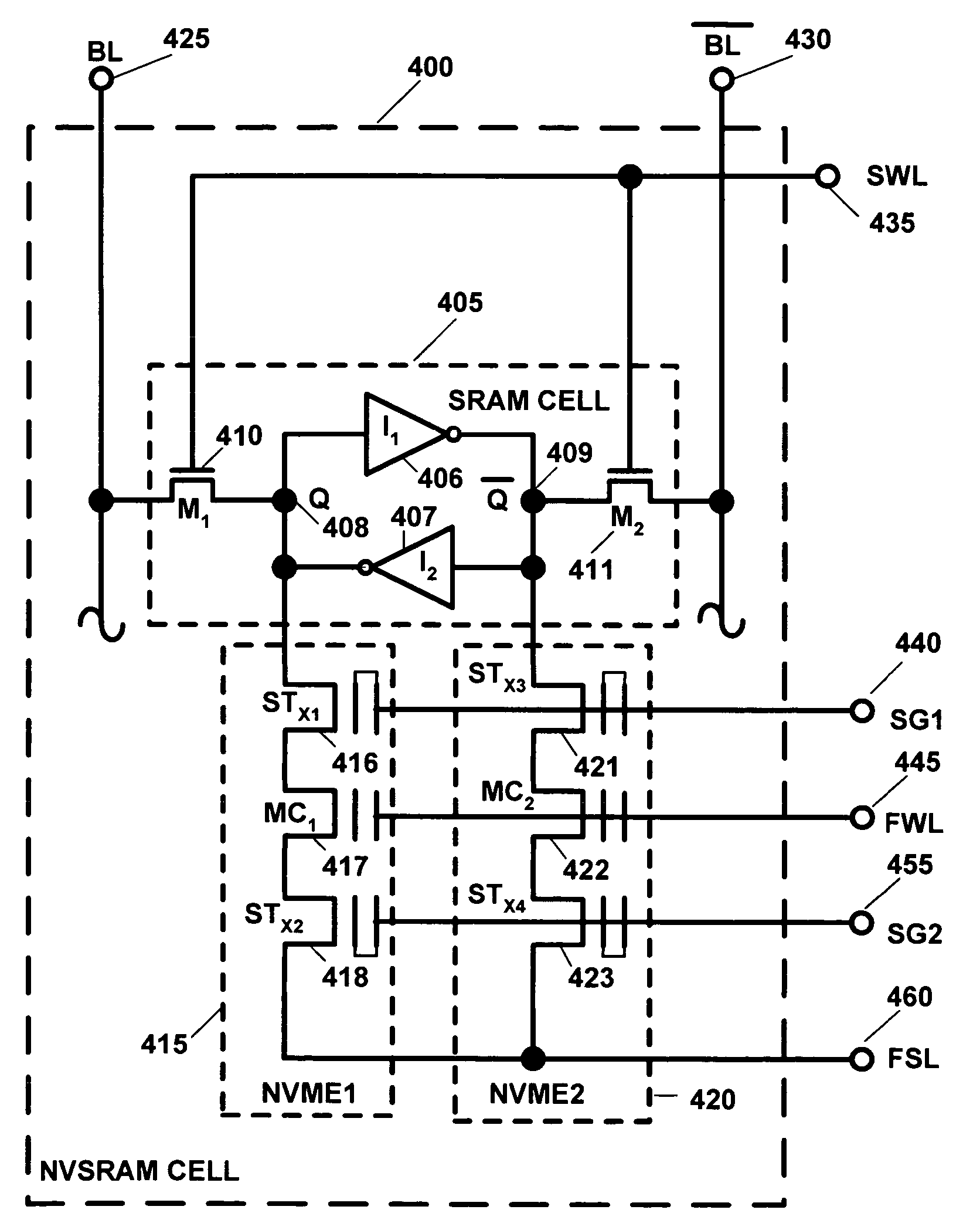
[0040]The Nonvolatile static random access memory (NVSRAM) circuit of this invention integrates an SRAM cell with nonvolatile memory elements. The NVSRAM circuit of this invention operates as a conventional SRAM, allowing for high-speed random read and write operations when VDD is turned on, but also as a flash cell that is capable of retaining the SRAM data upon interruption of the power supply voltage source VDD. The digital data is retained permanently within the NVSRAM circuit because the digital data is written into the nonvolatile memory elements. A power supply voltage source detection and control circuit provides the appropriate control signals to write the digital data retained within the SRAM cell to the nonvolatile memory elements within a predetermined period time upon detection of an interruption in the power supply voltage source VDD. The power supply voltage source detection and control circuit, upon detection of an initiation of the power supply voltage source, reads...


PUM


Abstract

A nonvolatile SRAM array has an array of integrated nonvolatile SRAM circuits arranged in rows and columns on a substrate. Each of the integrated nonvolatile SRAM circuits includes an SRAM cell, a first and second nonvolatile memory element. The SRAM cell has a latched memory element in communication first and second nonvolatile memory elements to receive and permanently retain the digital signal from the latched memory element. A power detection circuit detects a power interruption and a power initiation and communicates the detection of the power interruption and power initiation to the plurality of integrated nonvolatile SRAM circuits. The SRAM cell, upon detection of the power interruption, transmits the digital signal to the first and second nonvolatile memory elements. The SRAM cell of each of the nonvolatile static random access memories upon detection of the power initiation, receives the digital signal from the first and second nonvolatile memory elements.

Description

BACKGROUND OF THE INVENTION[0001]1. Field of the Invention[0002]This invention relates generally to a random access memory (RAM) circuits. More particularly, this invention relates to static RAM circuits. Even more particularly, this invention relates to integrated nonvolatile static RAM (NVSRAM) circuits.[0003]2. Description of Related Art[0004]Static random access memory (SRAM) is well known in the art and consists of a bistable transistor flip-flop or latching circuit. Referring to FIGS. 1a and 1b, the inverters I1 5 and I2 10 are coupled such that the output of the inverter I1 5 is connected to the input of the inverter I2 10 and the output of the inverters I2 10 is connected to the input of the inverter I1 5 to form the bistable latch. The access transistor Ma1 15 has a first source / drain terminal connected to the input of the inverter I1 5 and the output of the inverter I2 10 and a second source / drain terminal connected to the bit line BL 25. The access transistor Ma2 20 has a...

Claims


Application Information

Patent Timeline
Patent Type & Authority Patents(United States)
IPC IPC(8): G11C7/10
CPCG11C14/00G11C14/0063G11C16/10G11C11/41G11C16/00
Inventor LEE, PETER
Owner ABEDNEJA ASSETAB L L C
Why Eureka
Try Eureka