Optical transmitters and interconnects using surface-emitting lasers and micro-optical elements

a surface-emitting laser and optical transmitter technology, applied in semiconductor lasers, optical elements, instruments, etc., can solve the problems of difficult direct integration of vcsels to receiving detectors or optical fibers, significant optical aberration and insertion losses, and the difficulty of precise alignment that is necessary for integration to become an even bigger challenge. , to achieve the effect of improving the configuration of optical transmitters and interconnects, improving the flexibility and simplicity of optical design, fabrication and integration

Inactive Publication Date: 2007-01-16
ARMY US SEC THE
View PDF17 Cites 16 Cited by
  • Summary
  • Abstract
  • Description
  • Claims
  • Application Information

AI Technical Summary

Benefits of technology

[0010]This invention improves upon existing discrete and integrated vertical-cavity surface-emitting laser (VCSEL) fabrication techniques by providing an approach to hybridized structures including micro-optical elements (MOEs) monolithically incorporated into associated electronics for beam shaping to realize improved optical transmitters and interconnect configurations. Broadly, according to this invention, sub-micrometer-scale micro-optical elements (MOEs) are fabricated monolithically onto transparent driver substrates to achieve flexibility and simplicity in optical design, fabrication, and integration. In the preferred configurations, the VCSELs are hybridized onto MOE-bearing substrates using flip-chip bonding technique to form an integrated and optically controlled transmitter. The MOEs have optical functionalities of collimation or focusing according to specific application requirements.
[0013]Overall, the approach facilitates a simplified system that eliminates bulky conventional optical components and minimizes or eliminates the insertion loss and optical aberrations in other similar optical systems, thereby dramatically increasing the overall efficiency of the interconnect system.

Problems solved by technology

This property makes the direct integration of VCSELs to the receiving detectors or optical fibers very difficult since there is a large loss in device coupling.
For a two-dimensional system, a precise alignment that is necessary for the integration would become an even bigger challenge.
However, it has been found that excessive optical parts could cause significant optical aberrations and insertion losses and increase substantially the packaging costs.
The required monolithic fabrication process is also very complicated with little flexibility.
It is very difficult to integrate optical transmitters to the receiving detectors and optical fibers.
External optical components can be employed to shape the beams, but they will cause significant optical aberrations and insertion losses, increase packaging costs, and ultimately reduce the power efficiency.

Method used


Image

  • Optical transmitters and interconnects using surface-emitting lasers and micro-optical elements
  • Optical transmitters and interconnects using surface-emitting lasers and micro-optical elements
  • Optical transmitters and interconnects using surface-emitting lasers and micro-optical elements

Examples


Embodiment Construction

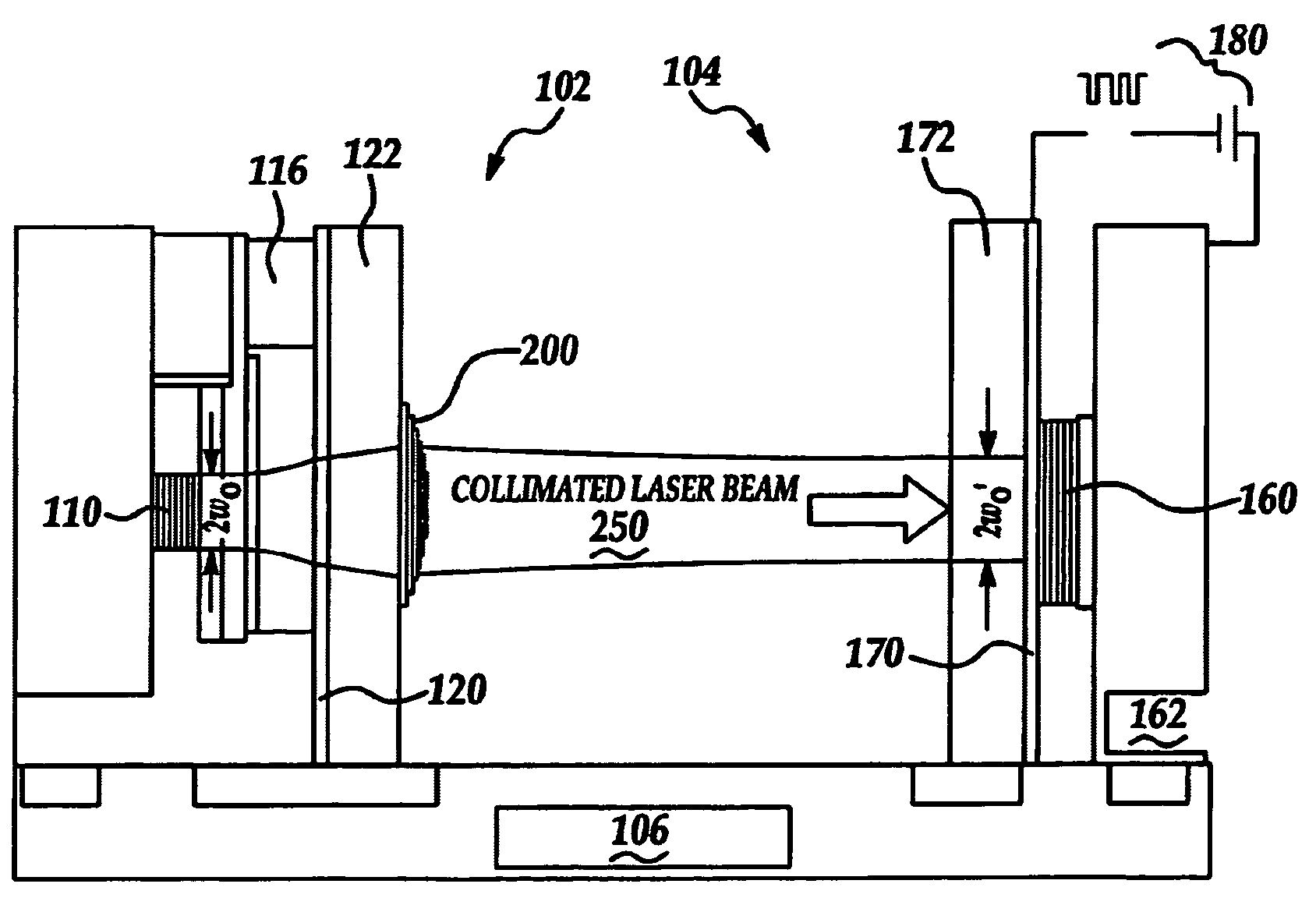
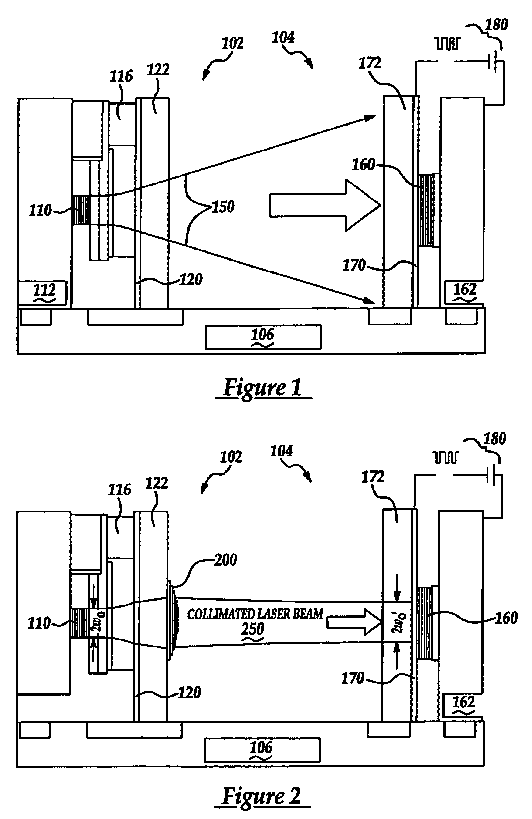
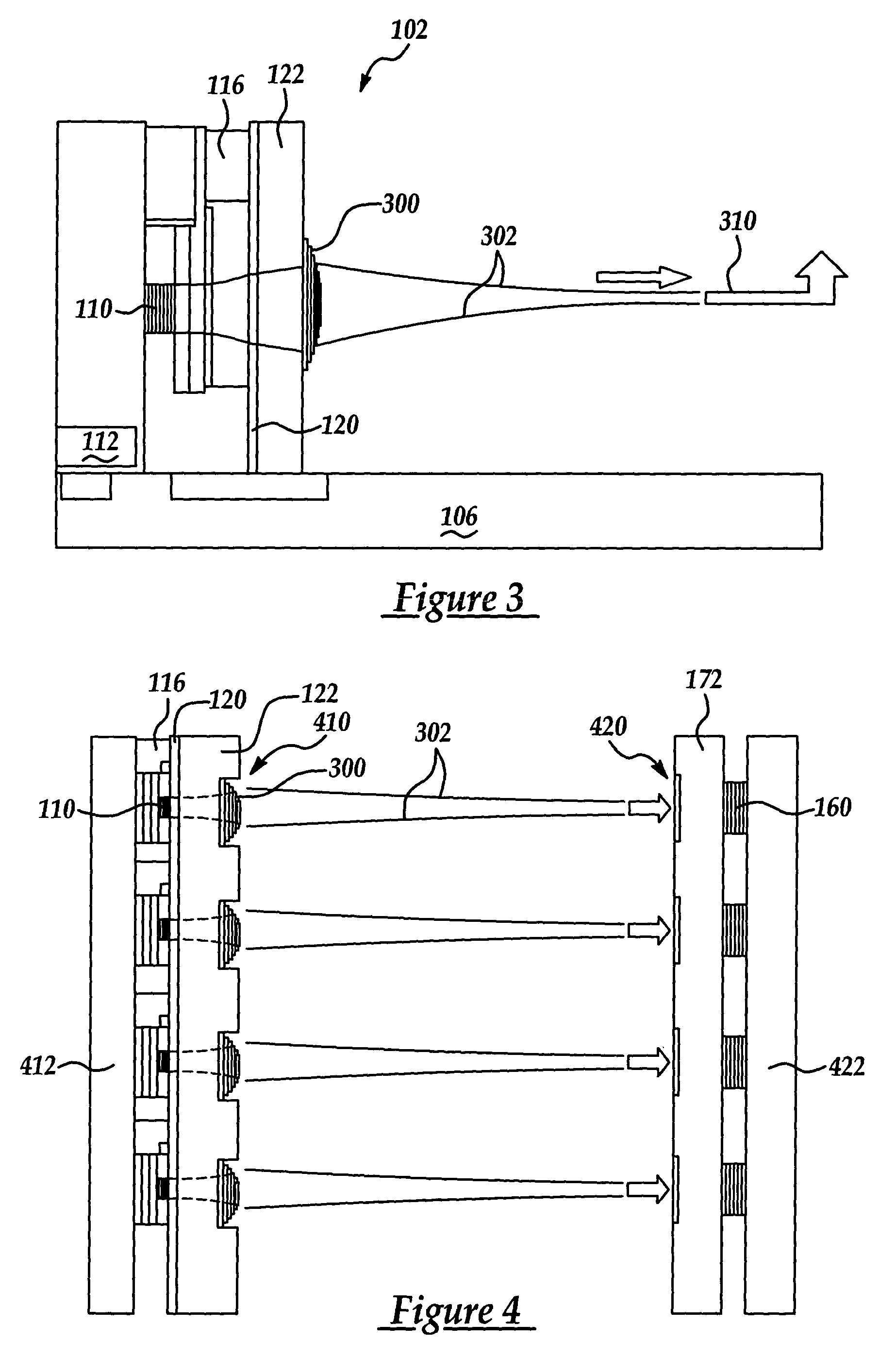
[0020]According to this invention, micro-optical elements (MOEs) are designed and fabricated onto transparent laser driver substrates to collimate or focus the beams from vertical-cavity surface-emitting lasers (VCSELs) in accordance with specific application requirements. According to a method aspect of the invention, the VCSELs are hybridized onto the MOE-bearing substrates using flip-chip bonding technique to form integrated and optically controlled transmitters.

[0021]In the preferred embodiments, silicon-on-sapphire (SOS) substrates are used in conjunction with complimentary metal-oxide-semiconductor (CMOS) VCSEL driver circuits. The driver circuits are fabricated on the sapphire substrates without affecting the optical transmission coefficient. Specifically, the sapphire driver substrates include a layer of index-matching material, and the MOE structures with specific functionality are fabricated on this index matching material using lithography and chemical etching processes. ...


PUM


Abstract

Micro-optical elements (MOEs) are designed and fabricated onto transparent laser driver substrates to collimate or focus the beams from vertical-cavity surface-emitting lasers (VCSELs) in accordance with specific application requirements. One disclosed example teaches the hybrid integration of a top-emitting 850 mm VCSEL array and a transparent sapphire substrate that supports a monolithic MOE with designated optical functionality. A flip-chipping hybridization technique ensures a realistic and reliable process. The VCSEL beams transmit directly through the MOE structure on the transparent sapphire substrate and become well-controlled optical outputs under precise specifications. The optical power loss in such a beam shaping process is minimized compared to configurations based on conventional optical components.

Description

GOVERNMENT INTEREST[0001]The invention described herein may be manufactured, used, and licensed by or for the United States Government.FIELD OF THE INVENTION[0002]This invention relates generally to vertical-cavity surface-emitting lasers (VCSELs) and, in particular, to devices and methods for integrating VCSELs and micro-optical elements (MOEs) to produce improved discrete and integrated structures.BACKGROUND OF THE INVENTION[0003]Vertical-cavity surface-emitting lasers (VCSELs) represent a new generation of high-speed, high-efficiency devices ideal for high-bandwidth optical sensors and data communication in military applications.[0004]VCSEL technology offers many advantageous properties, such as micro-scaled device size, two-dimensional scalability, and lower power consumption. As an optical transmitter, a VCSEL emits a beam having a Gaussian profile with an extremely large beam divergence (half angle of more than 15 degrees). This property makes the direct integration of VCSELs ...

Claims


Application Information

Patent Timeline
Patent Type & Authority Patents(United States)
IPC IPC(8): H01S5/00
CPCH01S5/423H01S5/02248G02B6/43G02B6/4206G02B6/4249H01S5/02325
Inventor LIU, JONY JIANGSIMONIS, GEORGE J.
Owner ARMY US SEC THE
Why Eureka
Try Eureka