Fabrication method for liquid crystal display

a liquid crystal display and fabrication method technology, applied in the direction of electrical equipment, semiconductor devices, instruments, etc., can solve the problems of relatively poor step coverage of the lcd substrate and relatively high directionality, and achieve the effect of enhancing operation and display quality, and reducing the r/c time delay

Active Publication Date: 2007-01-30
HANNSTAR DISPLAY CORPORATION
View PDF2 Cites 11 Cited by
  • Summary
  • Abstract
  • Description
  • Claims
  • Application Information

AI Technical Summary

Benefits of technology

[0013]Accordingly, the object of the invention is to provide a fabrication method for a liquid crystal display panel and a fabrication method for a liquid crystal display utilizing the same, for reducing R / C time delay to enhance the operation and display quality in large screen LCDs.
[0014]To achieve the object, the present invention provides a fabrication method for a liquid crystal display panel and a fabrication method for a liquid crystal display utilizing the same, wherein a gate metal may be deposited directly on a substrate using a patterned mask layer as a mask, and omitting subsequent steps of gate metal etching and polishing. When the method of the present invention is applied to a copper gate electrode process, R / C time delay caused by gate electrode material can be effectively reduced without requiring a special etching recipe, and inadequate yield due to poor polishing can be prevented.
[0015]Additionally, in the methods, the design of the opening of the hollow region of the mask pattern exhibits a geometric space with a relatively narrow top and a relatively wide bottom, that is, a reverse-tapered opening. The deposition of a metal layer on the LCD substrate is performed using a deposition with relatively poor step coverage and relatively high directionality. By designing the opening to have a narrow top and a wide bottom, the deposited metal in the vicinity of the top of the reverse-tapered opening forms an overhang structure. This structure, in turn, hinders the metal from further depositing on the corresponding bottom of the reverse-tapered opening, and, thus, the conductive line deposited on the bottom of the opening also has tapered sidewalls. The degree of the angle between the tapered sidewall and the panel substrate is not limited in the present invention and may be varied as desired.

Problems solved by technology

The deposition of a metal layer on the LCD substrate is performed using a deposition with relatively poor step coverage and relatively high directionality.

Method used


Image

  • Fabrication method for liquid crystal display
  • Fabrication method for liquid crystal display
  • Fabrication method for liquid crystal display

Examples


Embodiment Construction

[0023]A detailed description is given in the following embodiments with reference to the accompanying drawings.

[0024]In the present invention, a TFT LCD is fabricated. The TFT LCD comprises a TFT array substrate and a color filter substrate. Since the color filter substrate can be provided by any conventional color filter process, description thereof is omitted here.

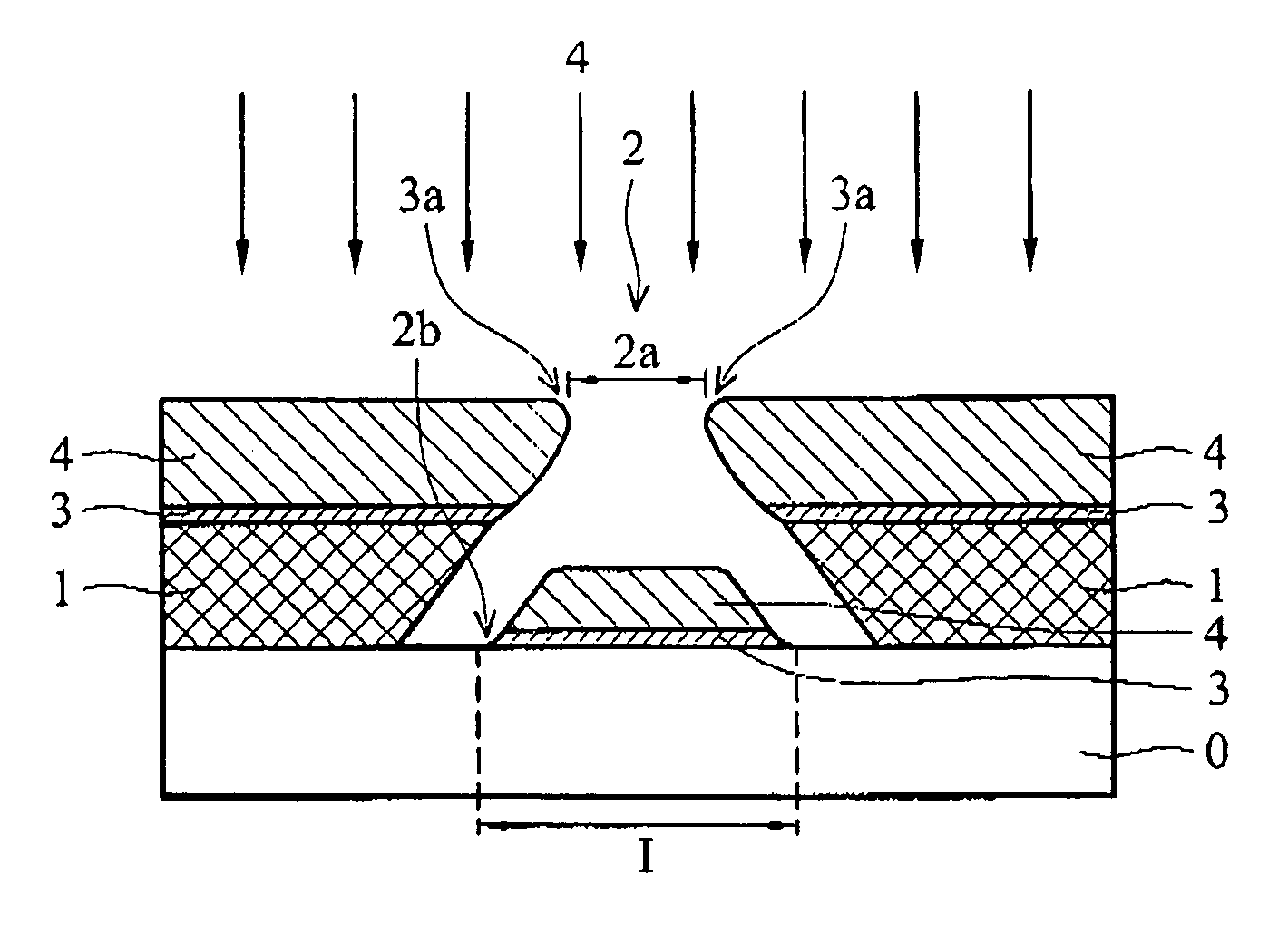
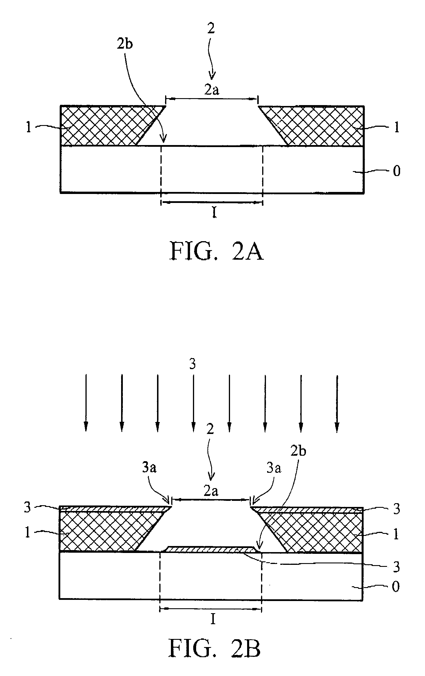
[0025]Referring to FIG. 2A, first, a substrate 0 is provided, which comprises a predetermined gate electrode area I. The substrate may comprise glass or light-transmissive plastic. The light-transmissive plastic may be polyethyleneterephthalate, polyester, polycarbonates, polyacrylates or polystyrene.

[0026]A mask layer 1 is formed on the substrate 0. The mask layer may be, for example a photoresist layer, preferably, a negative photoresist layer. In this embodiment, a negative photoresist layer is used. After soft baking and exposure of the pattern, the negative photoresist layer is cured by cross-linking. A development ...


PUM

PropertyMeasurementUnit
angleaaaaaaaaaa
angleaaaaaaaaaa
conductiveaaaaaaaaaa

Abstract

A method of fabricating a liquid crystal display panel is provided, which comprises the steps of providing a substrate; forming a mask layer over the substrate, wherein the mask layer has a reverse-tapered opening exposing a predetermined conductive line area; depositing a metal layer on the substrate within the predetermined conductive line area to form a conductive line with a tapered sidewall by performing an anisotropic deposition process; and removing the mask.

Description

BACKGROUND OF THE INVENTION[0001]1. Field of the Invention[0002]The present invention relates to a method of fabricating a liquid crystal display panel, and in particular to a method of forming conductive lines on a liquid crystal display substrate.[0003]2. Description of the Related Art[0004]Liquid crystal displays (LCDs) have gained widespread acceptance in the flat panel display market. Images are displayed by exploiting the photoelectric properties of liquid crystal layer, resulting from the arrangement conversion of liquid crystal upon being subjected to an external electric field, due to the dielectric anisotropy and conductive anisotropy of liquid crystal.[0005]The panel structure of a LCD typically comprises two laminated substrates with a gap therebetween, and liquid crystal injected into the gap. Corresponding electrodes on each substrate control the direction and arrangement of liquid crystal molecules.[0006]Currently, the development trend of flat panel display is toward...

Claims


Application Information

Patent Timeline
Patent Type & Authority Patents(United States)
IPC IPC(8): H01L21/00H01L21/336G02F1/1362H01L21/027H01L21/4763H01L29/423H01L29/49
CPCG02F1/136286H01L29/4908H01L29/42384H01L21/0272G02F2001/136295G02F1/136295
Inventor LEE, SHIH-WEICHANG, SHOU-JENFANG, YEN-WEN
Owner HANNSTAR DISPLAY CORPORATION
Why Eureka
Try Eureka