Method of manufacturing a split-gate flash memory device

a technology of split-gate flash memory and manufacturing method, which is applied in the direction of semiconductor devices, basic electric elements, electrical appliances, etc., can solve the problems of reducing the reliability of split-gate sonos memory, current leakage problem, etc., and achieve high etching selectivity and high reliability. yield

Active Publication Date: 2007-01-30
UNITED MICROELECTRONICS CORP
View PDF2 Cites 4 Cited by
  • Summary
  • Abstract
  • Description
  • Claims
  • Application Information

AI Technical Summary

Benefits of technology

[0014]It is therefore an objective of the present invention to provide a method of forming a split-gate flash memory to overcome the problems of the conventional method and enhance the reliability and the yield.
[0017]The flash memories produced using the method of the present invention have high reliability and yield. In addition, the doping process for the doping area is performed by utilizing the configurations of the dielectric layer which may be a photoresist layer or other film and the gate structures formed during the formation. Furthermore, the select gate is defined by the dielectric layer trimming process and utilizing the high etching selectivity of polysilicon to oxide. Therefore, the method of the present invention is also relatively simple and convenient.

Problems solved by technology

For example, a higher voltage difference between the word lines and the buried bit lines may be necessary when performing the erasing operation, or a current leakage problem may occur.
This leads to tunneling between the word lines and the buried bit lines, and reduces the reliability of split-gate SONOS memory.

Method used


Image

  • Method of manufacturing a split-gate flash memory device
  • Method of manufacturing a split-gate flash memory device
  • Method of manufacturing a split-gate flash memory device

Examples


Embodiment Construction

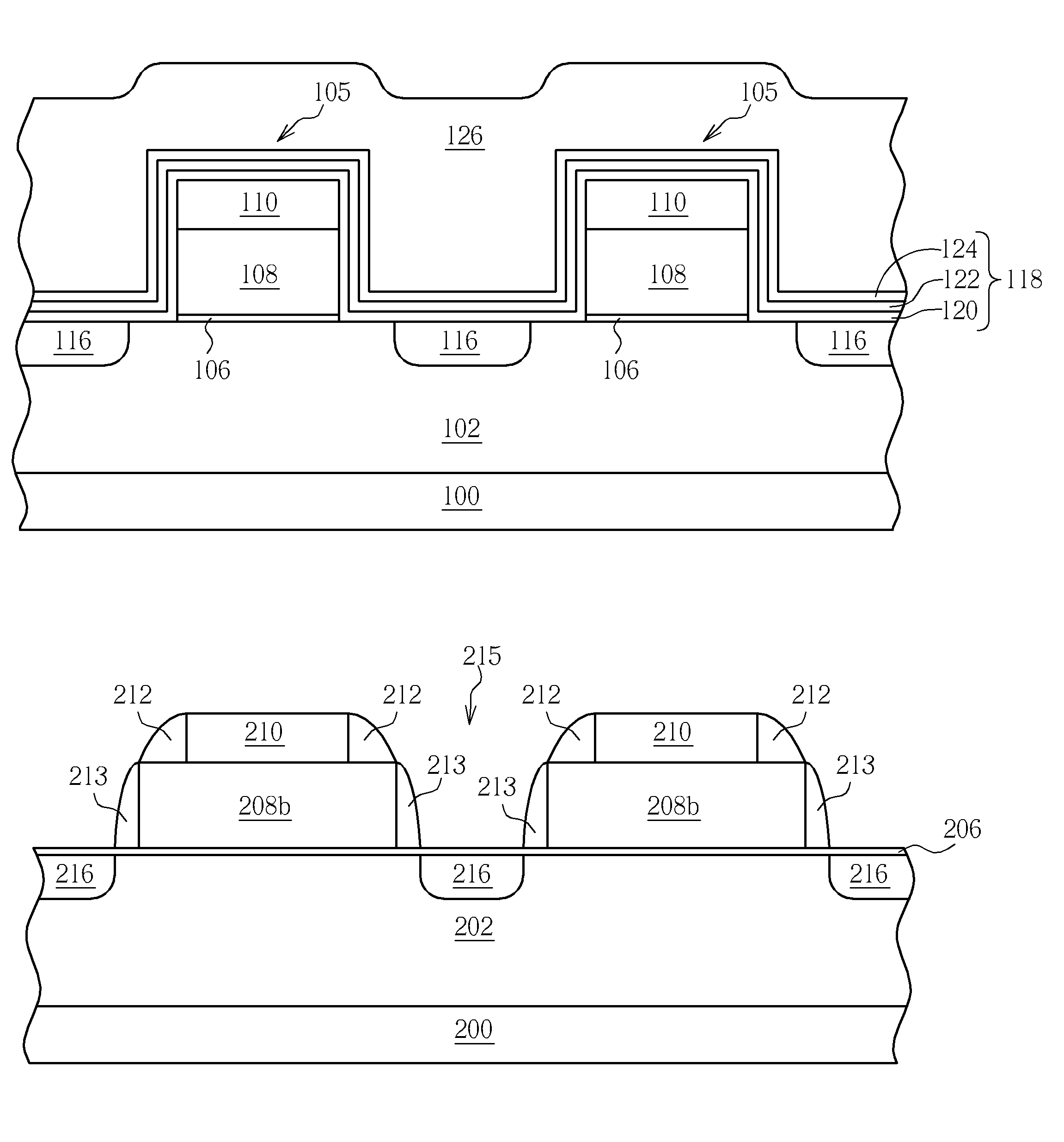
[0026]Please refer to FIG. 7 to FIG. 10. FIG. 7 to FIG. 10 are schematic diagrams illustrating a method of forming a split-gate flash memory according to a preferred embodiment of the present invention. It is to be appreciated that for emphasizing the defining characteristic of the present invention, FIG. 7 to FIG. 10 are cross-sectional views of some memory cells. As shown in FIG. 7, a semiconductor substrate 100 is provided, and at least a P well 102 is formed in the semiconductor substrate 100. The semiconductor substrate may be a P-type semiconductor substrate. Then, a polysilicon layer (not shown) serving as a conductive layer is formed on the semiconductor substrate 100 and patterned to form a plurality of parallel conductive lines 104. A gate insulating layer 106, such as an oxide layer, may be formed between the conductive lines 104 and the semiconductor substrate 100. The gate insulating layer 106 is a silicon oxide layer prepared by a thermal oxidization process or a depos...


PUM


Abstract

A method of manufacturing a split-gate flash memory device is disclosed. On a semiconductor substrate having a plurality of parallel conductive lines, a plurality of doped regions are formed by an ion implantation using the conductive lines as mask. Then, the conductive lines are trimmed for thinning the cover area. Afterward, a composite dielectric layer is formed on the substrate and covers the conductive lines. Finally, a plurality of word lines are formed on the composite dielectric layer.

Description

BACKGROUND OF INVENTION[0001]1. Field of the Invention[0002]The present invention relates to a method of forming a nonvolatile memory, and more particularly, to a method of forming a split-gate flash memory.[0003]2. Description of the Prior Art[0004]Nonvolatile memories have the advantages of maintaining stored data while the power supply is interrupted, and thus have been widely employed in recent years. According to the bit numbers stored by a single memory cell, nonvolatile memories are divided into single-bit storage nonvolatile memories, including nitride-based non-volatile memories such as Nitride Read-Only-Memory (NROM), Metal-Oxide-Nitride-Oxide-Silicon (MONOS) memories or Silicon-Oxide-Nitride-Oxide-Silicon (SONOS) memories, and dual-bit storage nonvolatile memories, such as split-gate SONOS memories and split-gate MONOS memories. Comparing to the traditional single-bit storage memories, the split-gate SONOS memories and split-gate MONOS memories are capable of storing more...

Claims


Application Information

Patent Timeline
Patent Type & Authority Patents(United States)
IPC IPC(8): H01L21/336
CPCH01L21/28282H01L27/11568H01L27/115H01L29/40117H10B43/30H10B69/00
Inventor YANG, MING-TZONGCHEN, TZU-PING
Owner UNITED MICROELECTRONICS CORP
Why Eureka
Try Eureka