Programming verification method of nonvolatile memory cell, semiconductor memory device, and portable electronic apparatus having the semiconductor memory device

a nonvolatile memory, semiconductor technology, applied in the direction of transistors, digital storage, instruments, etc., can solve the problems of inhibiting the microfabrication of the memory cell, difficult to effectively reduce the thickness of the gate insulating film, and difficult to suppress the short channel effect, etc., to achieve high affinity, facilitate discrimination, and suppress the effect of short channel

Active Publication Date: 2007-01-30
SHARP KK
View PDF12 Cites 17 Cited by
  • Summary
  • Abstract
  • Description
  • Claims
  • Application Information

AI Technical Summary

Benefits of technology

[0020]In the nonvolatile memory cell used in the programming verification method of the present invention, a memory function of the memory functional unit and a transistor operation function of the gate insulating film are separated from each other. Consequently, it is easy to suppress the short channel effect by thinning the gate insulating film while remaining the sufficient memory function. Further, a value of current flowing between the diffusion regions by rewriting changes larger as compared with the case of an EEPROM. Therefore, it facilitates discrimination between the writing state and the erasing state of the semiconductor memory device.
[0021]Further, the nonvolatile memory cell in the semiconductor memory device of the present invention can be formed by a process which has very high affinity with a normal transistor forming process on the basis of the configuration. Therefore, as compared with the case of using a conventional flash memory as a nonvolatile memory cell and forming the memory cell together with a peripheral circuit which is usually made by a transistor, the number of masks and the number of processes can be dramatically reduced. Consequently, the yield of a chip on which the memory cell and the peripheral circuit are formed together can be improved. Because of this, the manufacturing cost is reduced, and a very-reliable, cheap semiconductor memory device can be obtained.
[0031]According to the present invention, it is possible to provide the programming verification method of verifying that a memory cell having three or more possible states is written in a desired state without being under-programmed.
[0041]According to the present invention, it is possible to provide the programming verification method of verifying that a memory cell having three or more possible states is written in a desired state.
[0066]With the configuration, charges injected into the memory functional units increase and programming speed increases.
[0068]With the configuration, injection of charges into the memory functional units is facilitated and programming can be made at high speed.

Problems solved by technology

However, in the above-described flash memory, it has been functionally necessary to dispose the insulating film 907 for separating the floating gate 902 and the word line 903 from each other, and further, it has been difficult to reduce the thickness of the gate insulating film in order to prevent any leakage of charges from the floating gate 902.
As a consequence, it has been difficult to effectively reduce the thickness of each of the insulating film 907 and the gate insulating film, thereby inhibiting the microfabrication of the memory cell.

Method used


Image

  • Programming verification method of nonvolatile memory cell, semiconductor memory device, and portable electronic apparatus having the semiconductor memory device
  • Programming verification method of nonvolatile memory cell, semiconductor memory device, and portable electronic apparatus having the semiconductor memory device
  • Programming verification method of nonvolatile memory cell, semiconductor memory device, and portable electronic apparatus having the semiconductor memory device

Examples


first embodiment

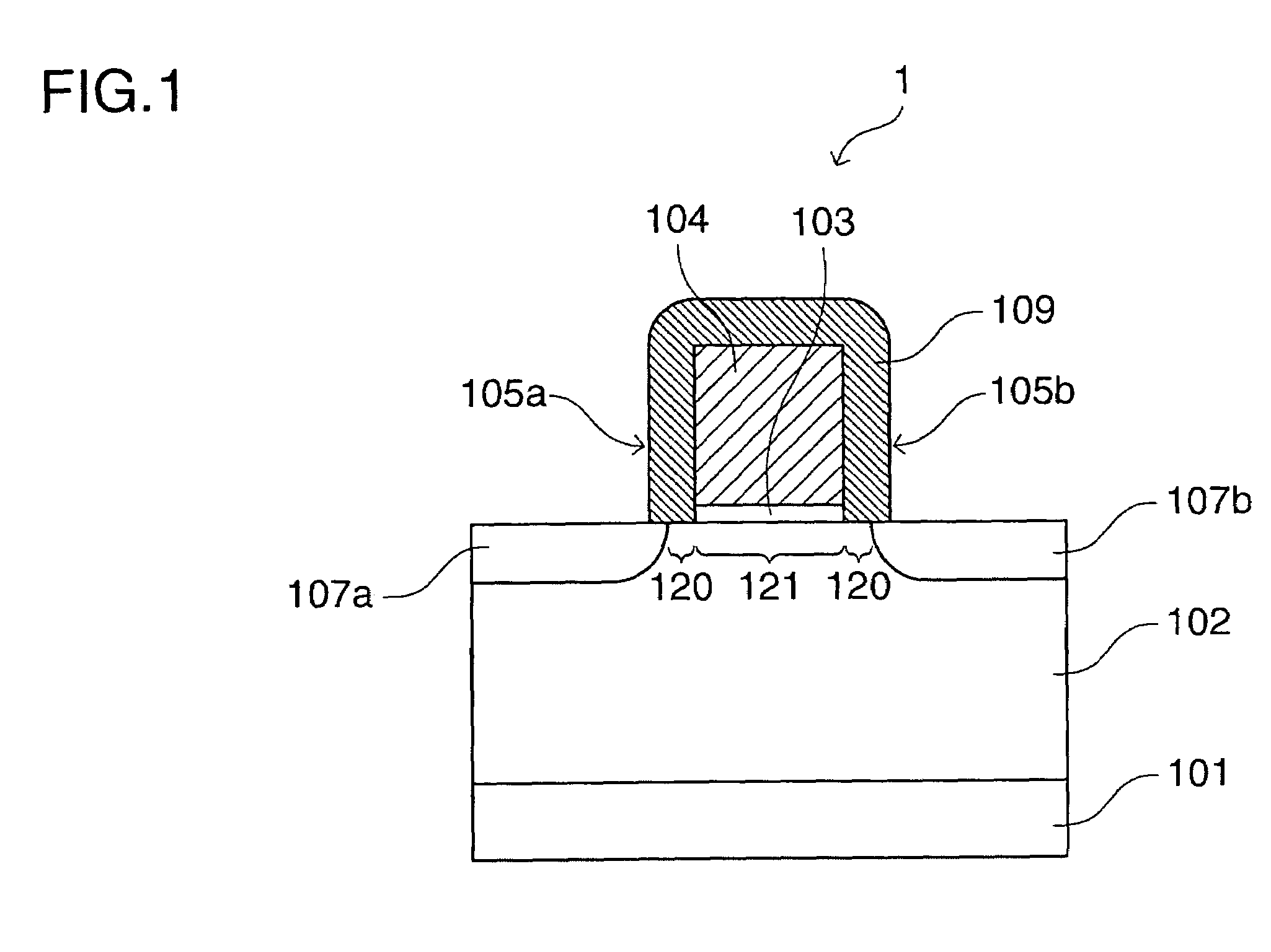
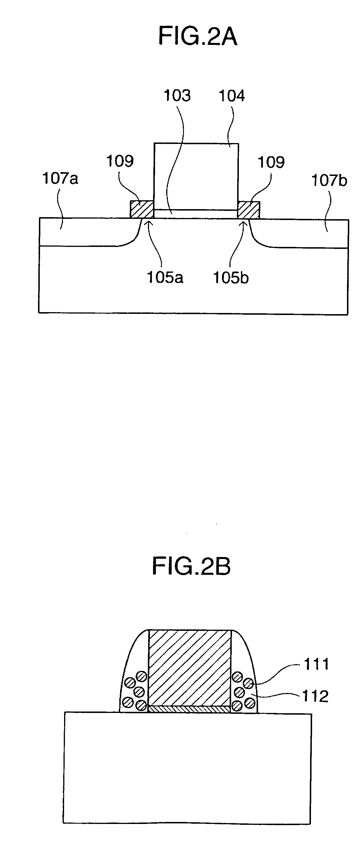
[0148]A semiconductor memory device of a first embodiment has a sidewall memory cell 1 as shown in FIG. 1.

[0149]The sidewall memory cell 1 has a gate electrode 104 formed on a P-type well region 102 formed on the surface of a semiconductor substrate 101 via a gate insulating film 103. On the top face and side faces of the gate electrode 104, a silicon nitride film 109 having a trap level of retaining charges and serving as a charge retaining film is disposed. In the silicon nitride film 109, parts of both sidewalls of the gate electrode 104 serve as memory functional units 105a and 105b for actually retaining charges. The memory functional unit refers to a part in which charges are actually accumulated by rewriting operation in the memory functional unit or the charge retaining film. In the P-type well region 102 on both sides of the gate electrode 104, N-type diffusion regions 107a and 107b functioning as a source region and a-drain region, respectively, are formed. Each of the dif...

second embodiment

[0169]A sidewall memory cell in a semiconductor memory device according to a second embodiment has a configuration substantially similar to that of the sidewall memory cell 1 of FIG. 1 except that, as shown in FIG. 8, each of memory functional units 261 and 262 is constructed by a charge retaining region (which is a charge accumulating region and may be a film having the function of retaining charges) and a region for suppressing escape of charges (or a film having the function of suppressing escape of charges).

[0170]From the viewpoint of improving a memory retention characteristic, preferably, the memory functional unit includes a charge retaining film having the function of retaining charges and an insulating film. In the second embodiment, a silicon nitride film 242 having a level of trapping charges is used as the charge retaining film, and silicon oxide films 241 and 243 having the function of preventing dissipation of charges accumulated in the charge retaining are used as ins...

third embodiment

[0186]The memory functional unit 262 in a semiconductor memory device of a third embodiment has a shape in which the silicon nitride film 242 as a charge retaining film has almost uniform thickness and is disposed almost in parallel with the surface of the gate insulating film 214 as shown in FIG. 13 (region 281) and, further, almost in-parallel with a side face of the gate electrode 217 (region 282).

[0187]In the case where positive voltage is applied to the gate electrode 217, an electric line 283 of force in the memory functional unit 262 passes the silicon nitride film 242 twice (regions 282 and 281) as shown by an arrow. When negative voltage is applied to the gate electrode 217, the direction of the electric line of force becomes opposite. Herein, the dielectric constant of the silicon nitride film 242 is about 6, and that of silicon oxide films 241 and 243 is about 4. Therefore, effective dielectric constant of the memory functional unit 262 in the direction of the electric li...


PUM


Abstract

A programming verification method of verifying programming of a nonvolatile memory cell, the method comprising at least the steps of: selecting first, second, . . . and n-th references corresponding to first, second, . . . and n-th threshold voltages specifying lower limit values of states 1, 2, . . . and n, respectively; applying a programming voltage to the nonvolatile memory cell; sensing a threshold voltage level of the nonvolatile memory cell; comparing the sensed threshold voltage level with the first reference to output a first result; comparing the threshold voltage level with one of the second and third references selected according to the first result to output a second result; and comparing the first and second results with an expectation value and, in the case where the first and second results are equal to the expectation value, indicating that the programming has succeeded, wherein the nonvolatile memory cell includes a gate electrode formed on a semiconductor layer via a gate insulating film, a channel region disposed under the gate electrode, a source and a drain as diffusion regions disposed on both sides of the channel region and having a conductive type opposite to that of the channel region, and memory functional units formed on both sides of the gate electrode and having the function of retaining charges.

Description

CROSS-REFERENCE TO RELATED APPLICATION[0001]This application is related to Japanese application No. 2003-142167 filed on May 20, 2003 whose priority is claimed under 35 USC § 119, the disclosure of which is incorporated by reference in its entirety.BACKGROUND OF THE INVENTION[0002]1. Field of the Invention[0003]The present invention relates to a programming verification method of a nonvolatile memory cell, a semiconductor memory device, and a portable electronic apparatus having the semiconductor memory device. More specifically, the present invention relates to a programming verification method or refreshing method of a memory cell including a memory functional unit having the function of retaining charges, a semiconductor memory device in which the memory cells are arranged, and a portable electronic apparatus having such a semiconductor memory device.[0004]2. Description of the Related Art[0005]Conventionally, a flash memory has been typically used as a nonvolatile memory.[0006]A...

Claims


Application Information

Patent Timeline
Patent Type & Authority Patents(United States)
IPC IPC(8): G11C16/06G11C16/02G11C11/22G11C11/34G11C16/04G11C16/34H01L21/28H01L21/336H01L21/8247H01L27/10H01L27/115H01L29/423H01L29/788H01L29/792
CPCG11C11/22G11C16/0475G11C16/3454G11C16/3459H01L29/7887H01L21/28282H01L29/42332H01L29/66825H01L29/66833H01L21/28273H01L29/40114H01L29/40117
Inventor IWASE, YASUAKIYAOI, YOSHIFUMIIWATA, HIROSHISHIBATA, AKIHIDEMORIKAWA, YOSHINAONAWAKI, MASARU
Owner SHARP KK
Why Eureka
Try Eureka