As is well known in the art, it is difficult to produce a completely flawless
active matrix liquid crystal display (LCD), when the display area is large, such as the LCD's on modem
laptop computers.
Single crystal silicon can be bonded to a glass substrate and then etched to remove most of the area to achieve transparency, but this is intrinsically wasteful in that, for the sake of maximizing
light transmission, the majority of the processed material is discarded and becomes
chemical waste.
The under-utilization of the precious die area wastes resources, causes greater amounts of
chemical waste to be generated in the process, and is generally inefficient and expensive.
Large arrays of silicon photodiodes with concentrating lenses have been made by sawing wafers and using a pick and place
assembly, but
thermal dissipation is poor for large elements, and the small elements require too much
assembly time.
These approaches avoid the limitations of the size of the available
single crystal silicon wafers, and avoid the cost of the
single crystal wafers, but require expensive deposition of the
semiconductor layer, and they still require
processing of the entire large substrate to form the active elements in an array, still resulting in the production of much
chemical waste and wasted resources.
These processes also limit the choice of the substrate; for example, plastic substrates cannot be used due to the nature of the processes which deposit the
semiconductor layers.
For displays, as an example, it is often difficult or impossible to form some of the desired circuitry out of the amorphous or
polycrystalline semiconductor materials.
Thus,
high frequency edge drivers may be impossible to form out of these materials.
As noted above, another difficulty with the existing techniques is that the large number of elements in a
large array results in a low probability that all of them will work properly and thus the yield of acceptably good arrays from the manufacturing process is low.
Furthermore, there is no possibility of testing any of the elements until the
assembly is complete, and then any imperfection in the array must be tolerated or the entire array could be discarded or special and expensive techniques must be used to repair it.
These problems result from the fact that the various elements in the array are fabricated on the array rather than separately.
Pick and place methods place devices generally one at a time, and are generally not applicable to very small or numerous elements such as those needed for large arrays, such as an
active matrix liquid crystal display.
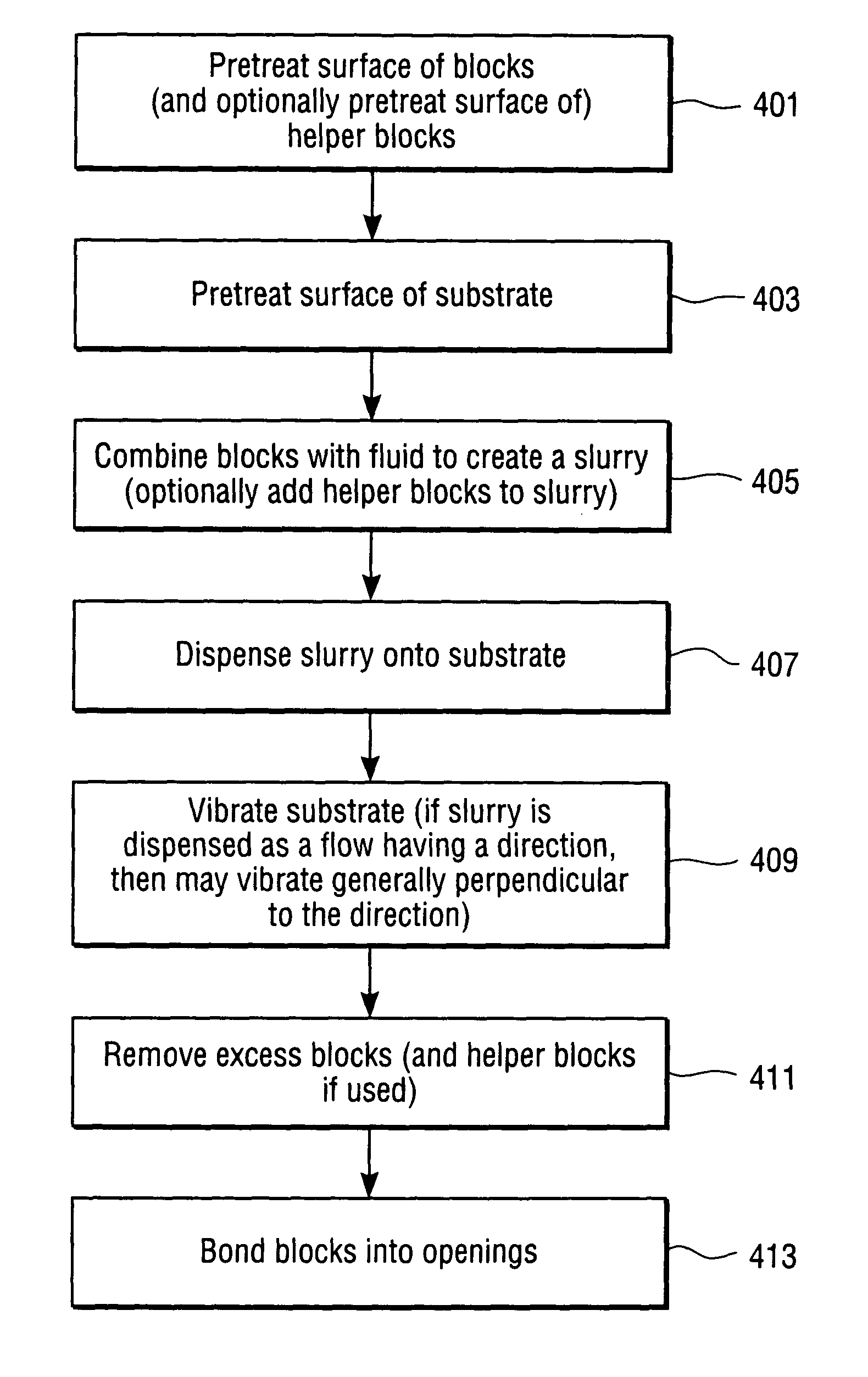
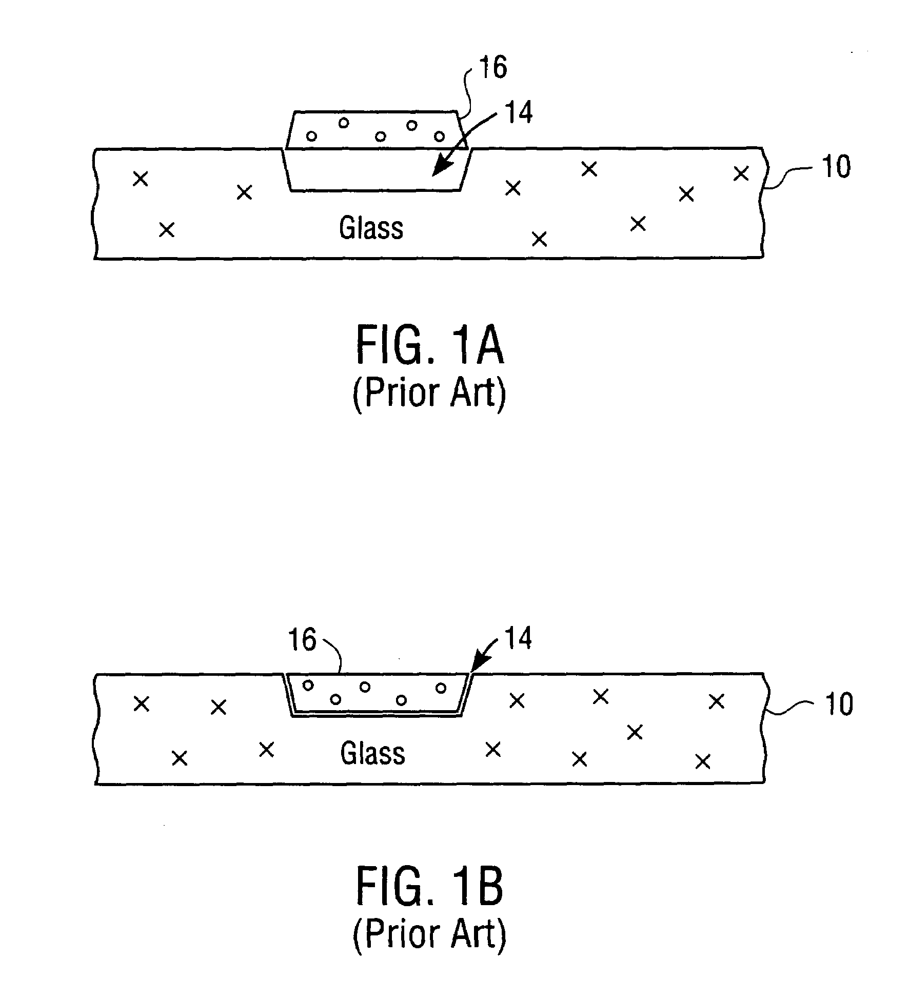
One issue in forming an opening is to create its sidewalls so that blocks will self-align into the opening and drop into the opening.
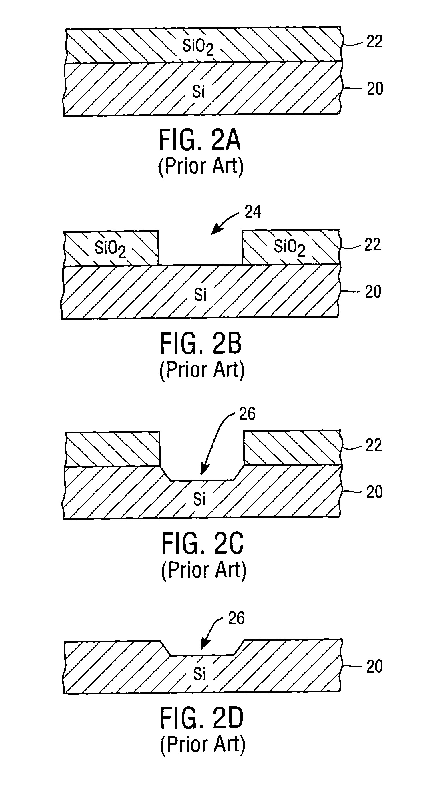
The structure shown in FIG. 2D has the drawback that a monocrystal silicon layer is required in order to use the KOH etch to form the hole.
While the foregoing methods allow an assembly to be created through a fluidic self-assembly process, these methods do not always provide perfect yields.
For example, the fluidic self-assembly process can still produce poor results if the elements do not flow smoothly over the service containing the openings.
Furthermore, the elements may become dislodged from the openings in subsequent
processing steps.

