

Field emission display having emitter arrangement structure capable of enhancing electron emission characteristics
- Summary
- Abstract
- Description
- Claims
- Application Information
AI Technical Summary
Benefits of technology
Problems solved by technology
Method used
Image

Examples
first embodiment
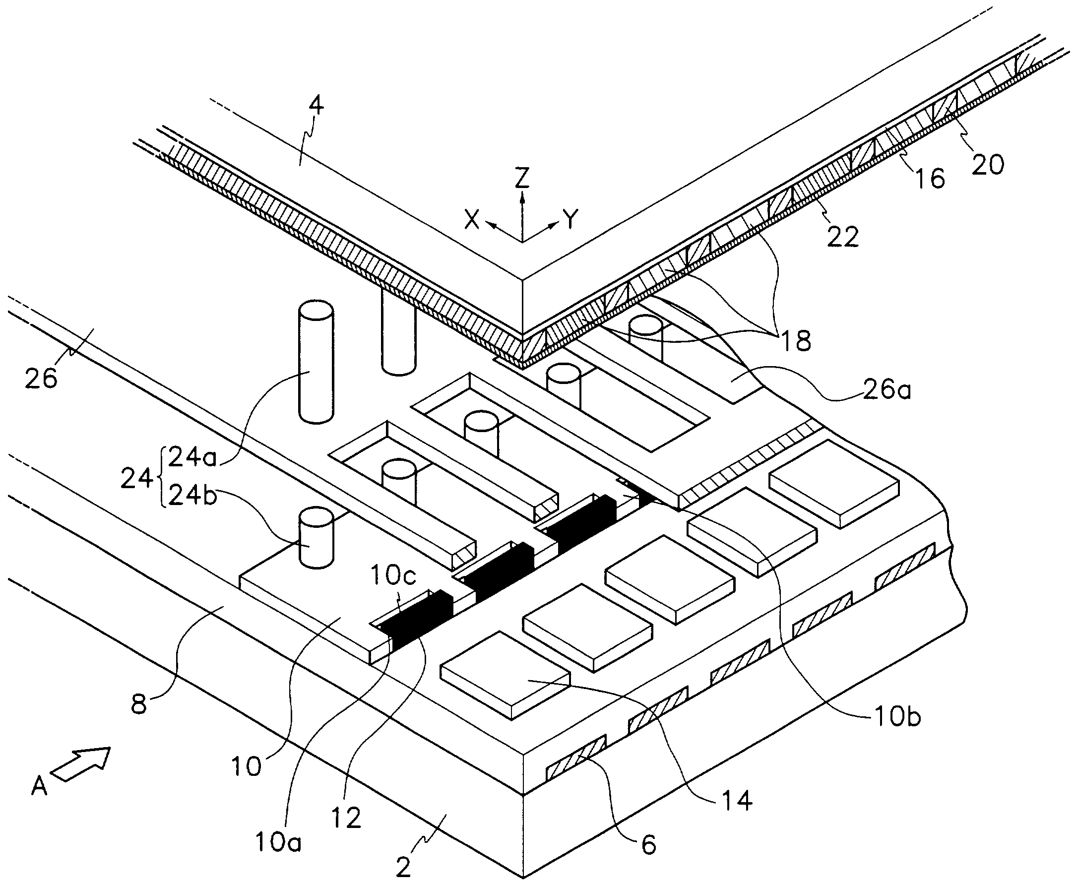
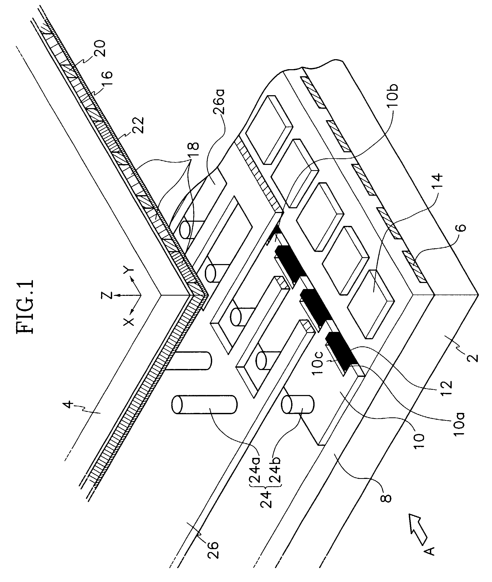
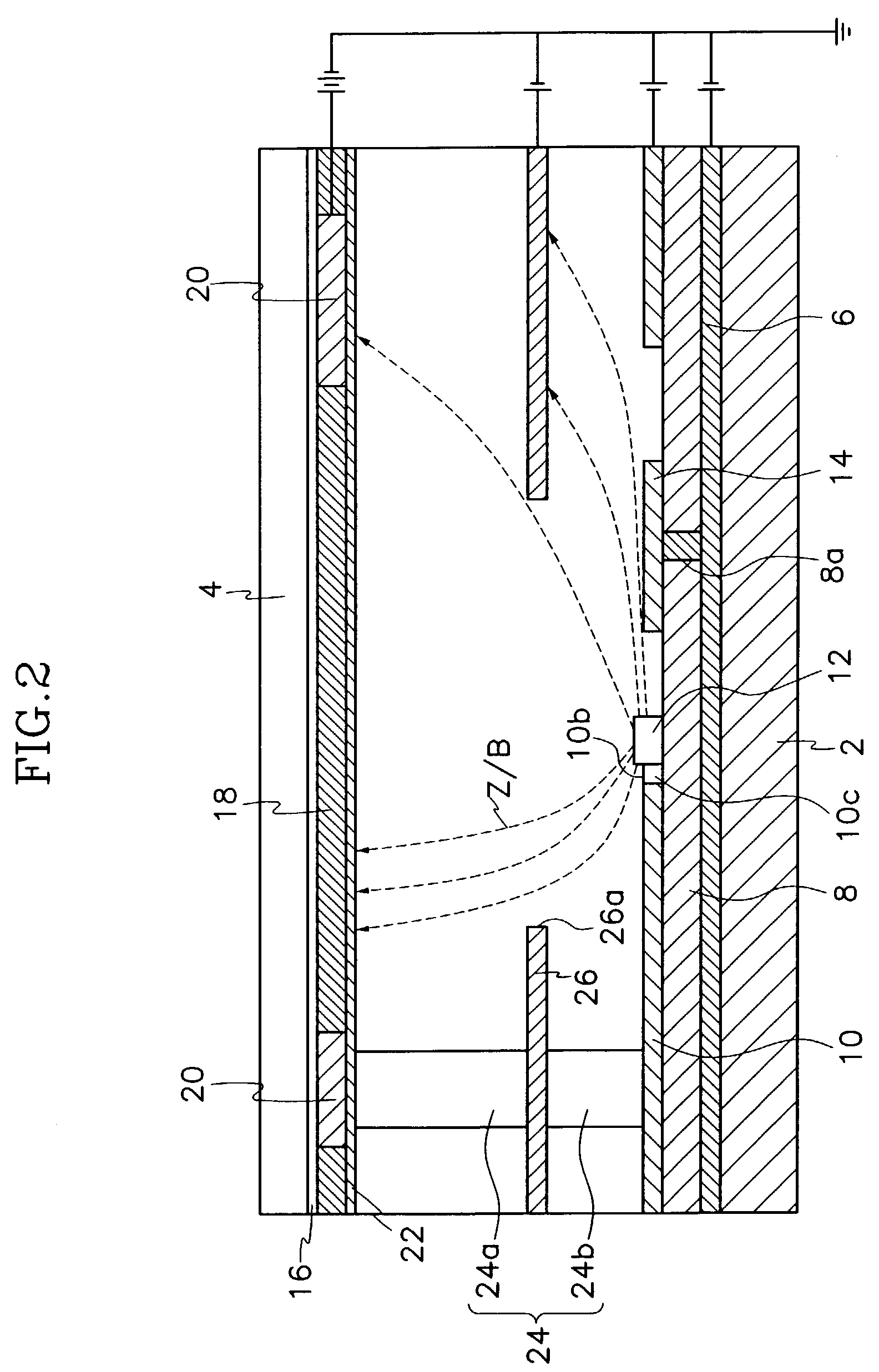
[0036]FIG. 1 is a partial perspective view of a field emission display according to the present invention, and FIG. 2 is a sectional view of the field emission display viewed from direction A of FIG. 1.
[0037]As shown in the drawings, the field emission display (FED) includes first substrate 2 of predetermined dimensions (hereinafter referred to as a rear substrate) and second substrate 4 of predetermined dimensions (hereinafter referred to as a front substrate). Front substrate 4 is provided substantially in parallel to rear substrate 2 with a predetermined gap therebetween, and front substrate 4 and rear substrate 2 are connected in this state to define an exterior of the FED.
[0038]A structure to enable the generation of an electric field is provided on rear substrate 2, and a structure to enable the realization of predetermined images by electrons emitted as a result of the generated electric field is provided on front substrate 4. This will be described in more detail below.
[0039...
second embodiment
[0065]In more detail, in the case where the emitters are formed directly over edges of the cathode electrodes (without the formation of emitter-receiving sections) as in conventional devices, the emission of electrons from the emitters varies depending on the area of the emitters. Such variations in the emission of the electrons may be particularly severe in the edges of the emitters. Emitters 40 according to the present invention act as resistance layers having resistivity such that voltage differences between gate electrodes 44 and cathode electrodes 42 at all areas of the edges of emitters 40 are the same. Therefore, the emission of electrons occurs evenly over all the edge portions of emitters 40.
[0066]At this time, it is possible for edges of emitters 40 closest to counter electrodes 46 to be aligned with corresponding edges of cathode electrodes 42. However, it is preferable for emitters 40 to be mounted more inwardly within emitter-receiving sections 42a as shown in FIG. 8 su...
PUM
 Abstract
Description
Claims
Application Information