Computer integrated manufacturing techniques

a technology of computer integrated manufacturing and manufacturing techniques, applied in the direction of total factory control, programme control, instruments, etc., can solve the problems of unavailability of required materials, unavailability of necessary maintenance replacement parts, and bottling or interruption, so as to facilitate processing or equipment changes, improve quality, yield and cost reduction

Inactive Publication Date: 2007-02-06
APPLIED MATERIALS INC
View PDF429 Cites 71 Cited by
  • Summary
  • Abstract
  • Description
  • Claims
  • Application Information

AI Technical Summary

Problems solved by technology

Effective inventory management of a wafer fab also requires a low incidence of bottlenecks or interruptions due to unscheduled down times which can for example be caused by unscheduled maintenance, interruptions resulting from processing parameters which are outside their specified limits, unavailability of required materials such as a process gas, unavailability of necessary maintenance replacement parts or unavailability of a processing tool such as a chamber.
However, it is recognized that a high degree of automation wherein various processes and metrologics are integrated, is difficult to achieve due to the complexity and inter dependency of many of the wafer fab processes, see for example Peter van Zandt, Microchip Fabrication, 3rd ed., McGraw-Hill, pp.
However, it is well known to those of ordinary skill in the art that a a commercial wafer fab typically includes semiconductor processing tools from different equipment manufacturers, resulting in tool compatibility difficulties when attempts are made to develop an integrated MES.
Scheduled downtime 106 occurs when the equipment is capable of performing its function but is not available to do this, such as process setup or preventive maintenance.
For example, if there is an error in the overlay or alignment of etch masks for interconnects in adjacent IC layers, the resulting interconnects are not in their proper design location.
This can result in interconnects which are packed too closely, forming electrical short defects between these interconnects.
It is also well known that two different processing problems can have a cumulative effect.
For example, a misalignment of interconnect etch masks which is not extensive enough to result in an electrical short, can still contribute to causing an electrical short if the process is slightly out of specification for allowing (or not detecting) particulate contamination having a particle size which would not have caused an electrical short if the interconnect masks had been in good alignment.

Method used


Image

  • Computer integrated manufacturing techniques
  • Computer integrated manufacturing techniques
  • Computer integrated manufacturing techniques

Examples


Embodiment Construction

[0036]While describing the invention and its embodiments, certain terminology will be utilized for the sake of clarity. It is intended that such terminology includes the recited embodiments as well as all equivalents.

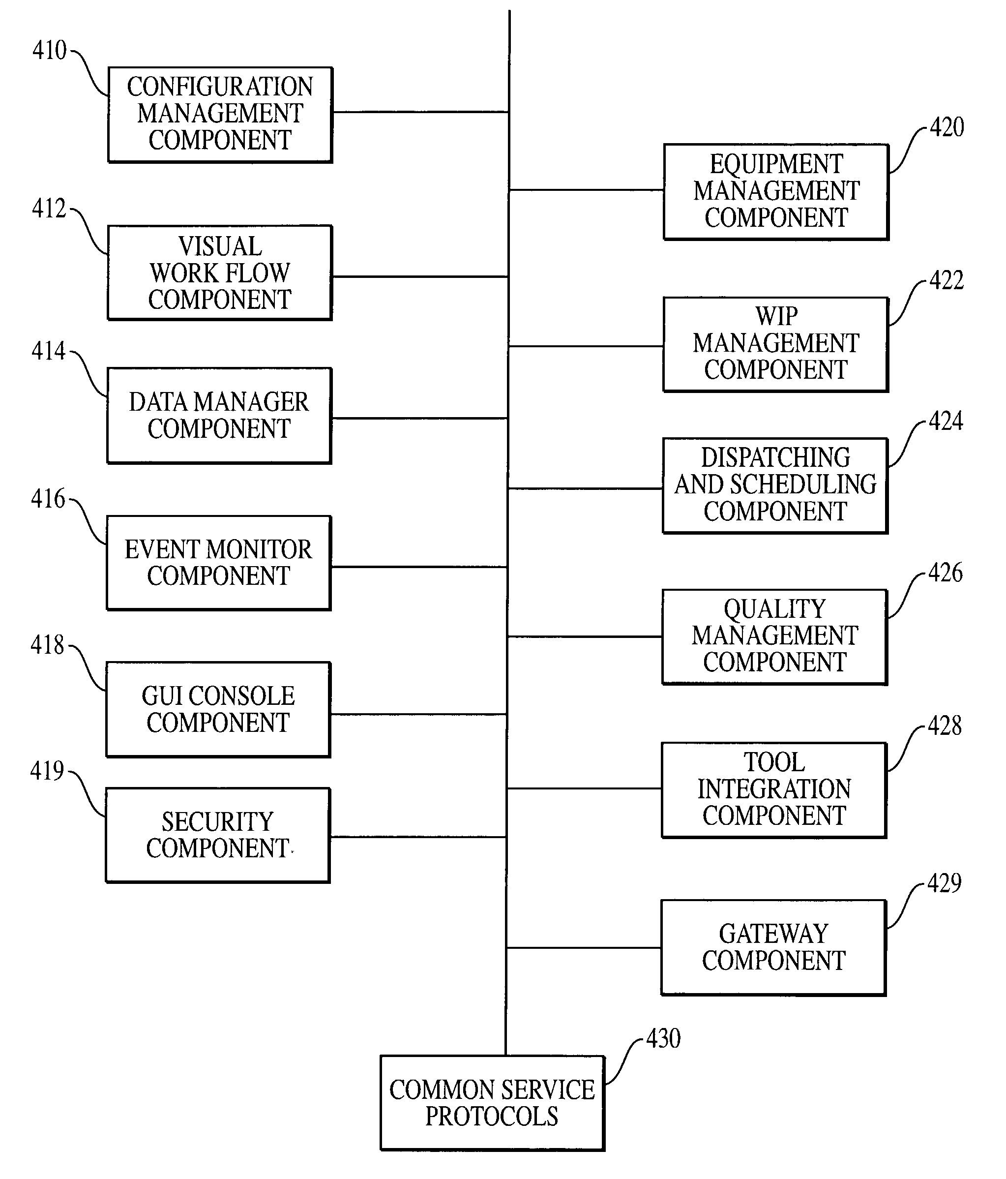
[0037]In one embodiment of the invention a DFS / F (distributed factory system framework) SW (software) environment is provided to automate, integrate and coordinate factory MES (manufacturing execution system(s)) comprising equipment steps, decision steps and data steps which can be present in a processing, manufacturing or fabricating system or facility such as a wafer fab for processing or fabricating semiconductor structures, such as IC (integrated circuit) structures. The expression “FW” (framework) as defined herein, includes a collection of linked SW structures, components or classes that provide a functionality or a set of services. The expression “MES” as defined herein, includes a collection of SW data structures for starting processing related tasks, managing a...


PUM


Abstract

The present invention provides a novel distributed factory system framework including a novel factory automation lifecycle (200) having lifecycle activities for SW developing and integrating (210), installing and administrating (220), factory modeling (230), manufacturing planning (240), manufacturing controlling, monitoring and tracking (250) and analyzing of manufacturing results (260). The factory lifecycle comprises framework components. The distributed factory system framework also includes application components and building blocks. The framework components are adapted to for managing the application components, while the application components are utilized to provide instructions for managing a process such as a wafer fab. The building blocks are adapted for forming or modifying framework and application components. The distributed factory system framework provides computer implemented methods for integrating processing systems and facilitates process and equipment changes.

Description

RELATED APPLICATIONS[0001]This application is a divisional of U.S. application Ser. No. 09 / 363,966, filed Jul. 29, 1999, which is incorporated herein by reference.GOVERNMENT RIGHTS IN THE INVENTION[0002]This invention was made with United States Government support under Cooperative Agreement No. 70NANB7H3043 awarded by NST. The United States Government has certain rights in the invention.FIELD OF THE INVENTION[0003]The present invention relates to techniques for computer integrated manufacturing.BACKGROUND OF THE INVENTION[0004]A semiconductor device such as an IC (integrated circuit) generally has electronic circuit elements such as transistors, diodes and resistors fabricated integrally on a single body of semiconductor material. The various circuit elements are connected through conductive connectors to form a complete circuit which can contain millions of individual circuit elements. Integrated circuits are typically fabricated from semiconductor wafers in 20 a process consistin...

Claims


Application Information

Patent Timeline
Patent Type & Authority Patents(United States)
IPC IPC(8): G06F19/00G05B19/418G06Q50/00H01L21/00H01L21/02
CPCG05B19/41845G05B2219/45026G05B2219/31202G05B2219/31018Y02P90/02Y02P90/80H01L21/00
Inventor ARACKAPARAMBIL, JOHN F.CHI, TOMCHOW, BILLYD'SOUZA, PATRICK M.HAWKINS, PARRISHUANG, CHARLESJENSEN, JETTKRISHNAMURTHY, BADRI N.KULKARNI, PRADEEP M.KULKARNI, PRAKASH M.LIN, WEN FONGMOHAN, SHANTHANANDY, BISHNUYUAN, HUEY-SHIN
Owner APPLIED MATERIALS INC
Why Eureka
Try Eureka