Method for fabricating connection terminal of circuit board

a technology of connection terminals and circuit boards, which is applied in the direction of contact member manufacturing, conductive pattern formation, non-metallic protective coating applications, etc., can solve the problems of increasing production costs, creating bottlenecks in process, amount and shape of solder materials used in the next printing, and not meeting the specifications of the design specification. , to achieve the effect of reducing yield, increasing fabrication complexity and cos

Active Publication Date: 2007-02-13
PHOENIX PRECISION TECH CORP
View PDF4 Cites 20 Cited by
  • Summary
  • Abstract
  • Description
  • Claims
  • Application Information

AI Technical Summary

Benefits of technology

[0015]A further objective of the present invention is to provide a method for fabricating connection terminals of the circuit board so as to prevent problems such as reduced yield, and increased fabrication complexity and cost caused by multiple deposition and removal of the resist and conductive layer in the conventional electroplating process for forming the connection terminals.
[0016]One other objective of the present invention is to provide a method for fabricating connection terminals of the circuit board so as to resolve problems such as size limitation posed by conventional template printing technique for forming the connection terminals, increased cost, and bottleneck in terms of fabrication technique.
[0018]According to the present invention, the method for fabricating connection terminals of the circuit board that is covered with an insulating layer having a plurality of first openings to expose the conductive pads formed thereon, which is characterized by forming a first patterned resist layer on the surface of the circuit board, electroplating a metal connection layer of predetermined height on the in the second openings. That is, the metal connection material of relatively lower height is electroplated on the connection pads of the circuit board. Then, a second patterned resist layer is formed to selectively expose a part of the first metal connection layer (for example, solder material for subsequently attaching to corresponding metal bumps of the flip-chip electrode pads). Since said metal connection layer for attaching to the flip-chip electrode pads is higher than the metal connection layer for surface mounting and solder ball attachment, it is necessary to have the third openings for further electroplating with the metal connection material. After the resist layers are removed, the metal connection material is subjected to reflow soldering process so as to form connection terminals of different heights. Therefore, the present invention also prevents problems such as damage to the connection terminals, reduced yield for the circuit board, and increased fabrication complexity and cost caused by multiple formation and removal of the resist layer and conductive layer when the connection terminals are formed successively by the conventional electroplating technique. In addition, the present invention resolves problems such as size limitation posed by conventional template printing technique for forming the connection terminals, increased cost, and bottleneck in terms of fabrication technique.

Problems solved by technology

These dynamic changes have brought in many challenges for package technology of the semiconductor chip.
So, the production cost is increased due to difficulty in the template development.
It is also difficult for the soldering material to pass through the minimized openings of the template, creating bottleneck in terms of the process.
As a result, the amount and shape of the solder material used in the next printing will not match those according to the designed specification.
In the actual operation, the template would have to be wiped clean after being applied to printing for certain number of times. Otherwise, it is very likely to create mismatched shape and size of the soldering material, causing process inconvenience and reduced reliability.
If the solder material of different heights and sizes were formed, the overall fabrication time and cost would be increased.
And the solder material that is formed as previously described may be loosened as a result of multiple formation and removal of the electroplating mask layer and conductive layer in the separate processes, resulting a drop in the circuit board yield.
Despite of exposure and development being common steps in the semiconductor IC substrate process, a highly viscous resist resin, special spin coater, and aligner with longer wavelength are used when the resist layer used in the electroplating process has a thickness of about 25 μm, resulting an increase in fabrication cost.

Method used


Image

  • Method for fabricating connection terminal of circuit board
  • Method for fabricating connection terminal of circuit board
  • Method for fabricating connection terminal of circuit board

Examples


Embodiment Construction

[0025]The present invention is described in the following with specific embodiments, so that one skilled in the pertinent art can easily understand other advantages and effects of the present invention from the disclosure of the invention. The present invention may also be implemented and applied according to other embodiments, and the details may be modified based on different views and applications without departing from the spirit of the invention.

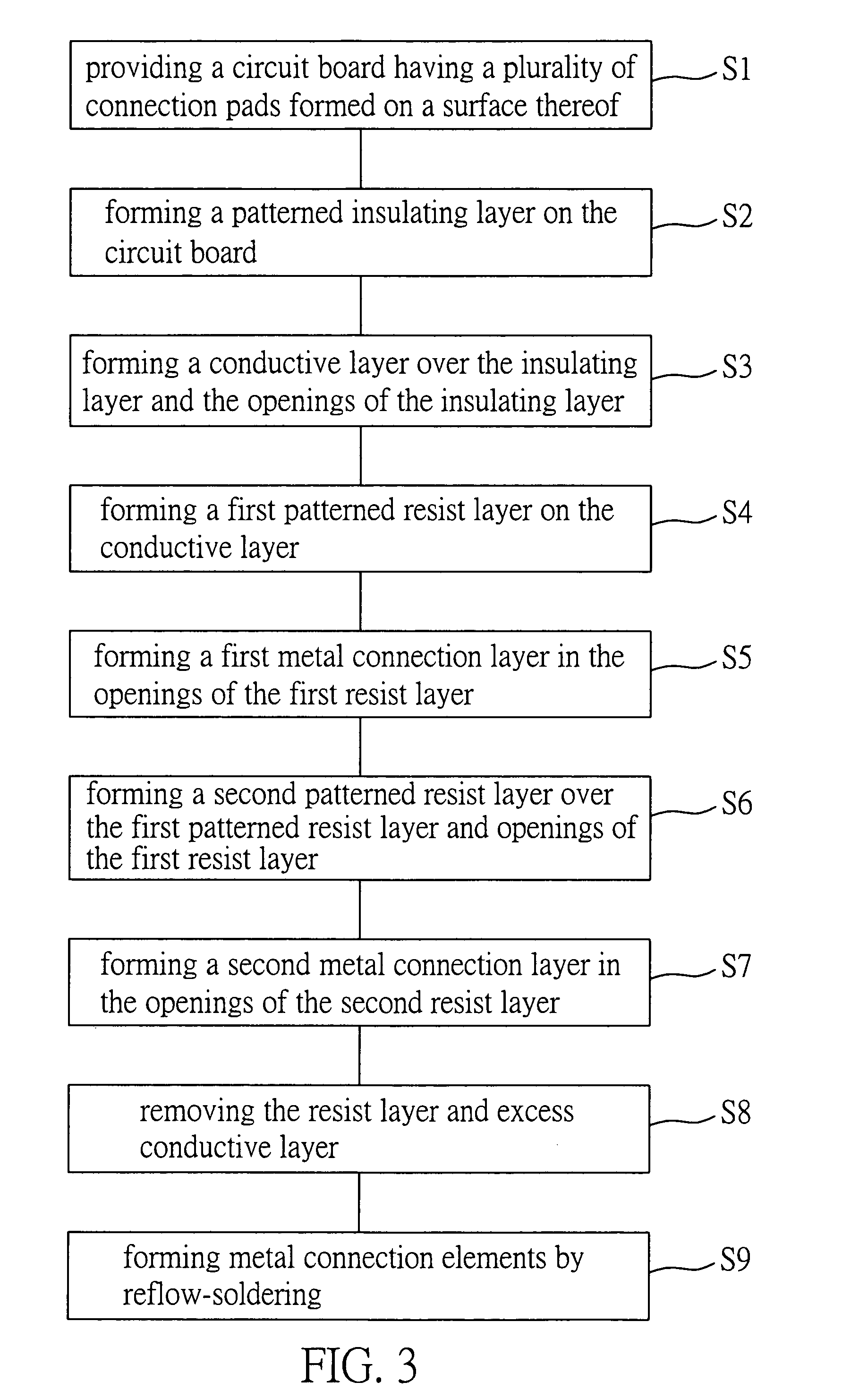
[0026]Referring to FIG. 3 for illustrating a method of fabricating the connection terminals of the circuit board according to the present invention, and in accompany with the cross-sectional views of the fabrication process illustrated in FIGS. 4A through to 4I, so as to describes the embodiments of the invention.

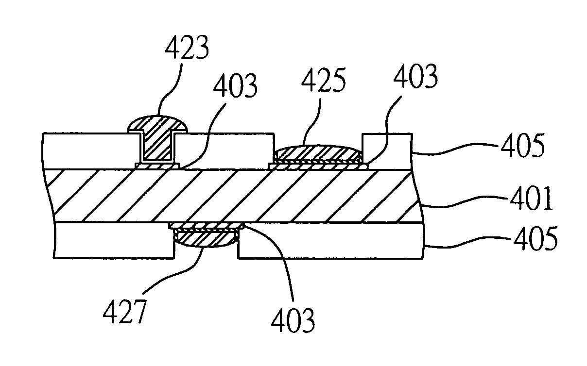
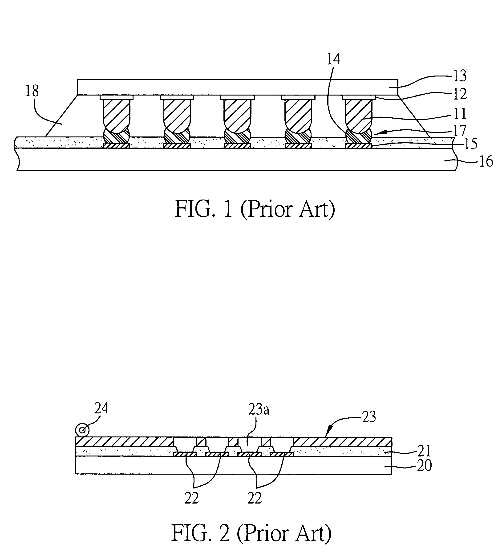
[0027]In step S1, a circuit board 401 having a plurality of connection pads 403 formed thereon (shown in FIG. 4A) is provided. The connection pads 403 may be metal connection pads for connecting to the metal bumps of the flip-c...


PUM

PropertyMeasurementUnit
thicknessaaaaaaaaaa
conductiveaaaaaaaaaa
heightsaaaaaaaaaa

Abstract

A method for fabricating connection terminals of a circuit board is proposed. The method involves providing a circuit board with connection pads thereon, forming an insulating layer with first openings over the circuit board to expose the connection pads, forming a conductive layer over the insulating layer, forming a first resist layer with second openings over the conductive layer to partially expose the conductive layer, electroplating a first metal connection layer on the exposed conductive layer, followed by forming a second resist layer with third openings over the first conductive layer to partially expose the first metal connection layer, and electroplating a second metal connection layer on the exposed first connection layer, and removing portions of the first and second resist layers and conductive layer covered by the first and second resist layers to form metal connection material of different heights and sizes on the connection pads.

Description

BACKGROUND OF THE INVENTION[0001]1. Field of the Invention[0002]The invention relates to a method for fabricating connection terminals of a circuit board, and more particularly, to a method for fabricating metal connection materials of different heights and sizes simultaneously on connection pads of the circuit board.[0003]2. Description of the Related Art[0004]In the recent years, electrical products such as notebook (NB) computer, mobile phone, personal digital assistant (PDA), and digital camera are developed in a more and more compact size while their operation speeds are getting faster by demands. These dynamic changes have brought in many challenges for package technology of the semiconductor chip. As the product designs are directed towards achieving minimization, high speed and multi-functions, flip-chip technique has been more widely applied as a standard chip packaging technique. And passive devices, such as resistors, capacitors, and inductors are formed in those electric...

Claims


Application Information

Patent Timeline
Patent Type & Authority Patents(United States)
IPC IPC(8): H01R9/00
CPCH05K3/243H01L2224/11474Y10T29/49155H05K3/28H05K3/3473H05K2201/0391H05K2201/09436H05K2203/043H05K2203/054H05K2203/0574H01L2224/11902Y10T29/49117Y10T29/49156Y10T29/49128Y10T29/49204Y10T29/49165Y10T29/49147H01L2924/00014H01L2224/05599H01L2224/0555H01L2224/0556H01L2224/0554H01L2224/05568H01L2224/05573H01L2224/11462
Inventor HSU, SHIH-PINGTANG, SAO-HSIASHIH, CHAO-WEN
Owner PHOENIX PRECISION TECH CORP
Why Eureka
Try Eureka