Method of fabricating liquid crystal display device

a liquid crystal display and display device technology, applied in semiconductor devices, electrical devices, instruments, etc., can solve problems such as deficiency in the liquid crystal display device, and achieve the effect of preventing a hangover of an organic passivation layer and simplifying the fabrication process

Active Publication Date: 2007-02-20
LG DISPLAY CO LTD
View PDF16 Cites 13 Cited by
  • Summary
  • Abstract
  • Description
  • Claims
  • Application Information

AI Technical Summary

Benefits of technology

[0023]Another object of the present invention is to provide a method of fabricating a liquid crystal display device capable of simplifying the fabrication process by exposing a pad by removing an organic passivation layer on the edge region of a liquid crystal panel.
[0024]Another object of the present invention is to provide a method of fabricating a liquid crystal display device capable of preventing a hangover of an organic passivation layer between pads in removing the organic passivation layer by differentiating the widths of slits formed at a slit portion of a diffraction mask or differentiating shapes of slits.

Problems solved by technology

However, in the use of the diffraction mask, problems that occur will be described as follows.
However, because interfacial characteristics between the metal layer 48 and the organic material are poor, the metal layer 48 is separated from the organic passivation layer 32 in forming of the metal layer 48, and accordingly deficiency occurs in the liquid crystal display device.

Method used


Image

  • Method of fabricating liquid crystal display device
  • Method of fabricating liquid crystal display device
  • Method of fabricating liquid crystal display device

Examples


Embodiment Construction

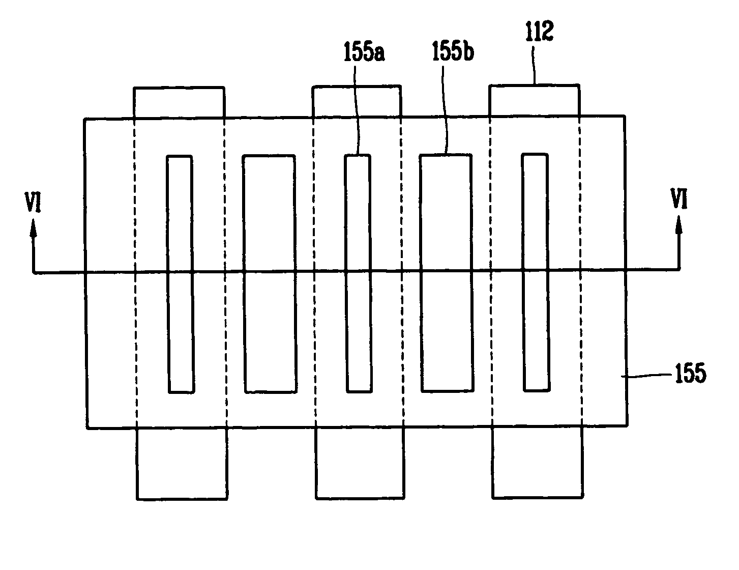
[0039]Reference will now be made in detail to the illustrated embodiments of the present invention, examples of which are illustrated in the accompanying drawings. Wherever possible, the same reference numbers will be used throughout the drawings to refer to the same or like parts.

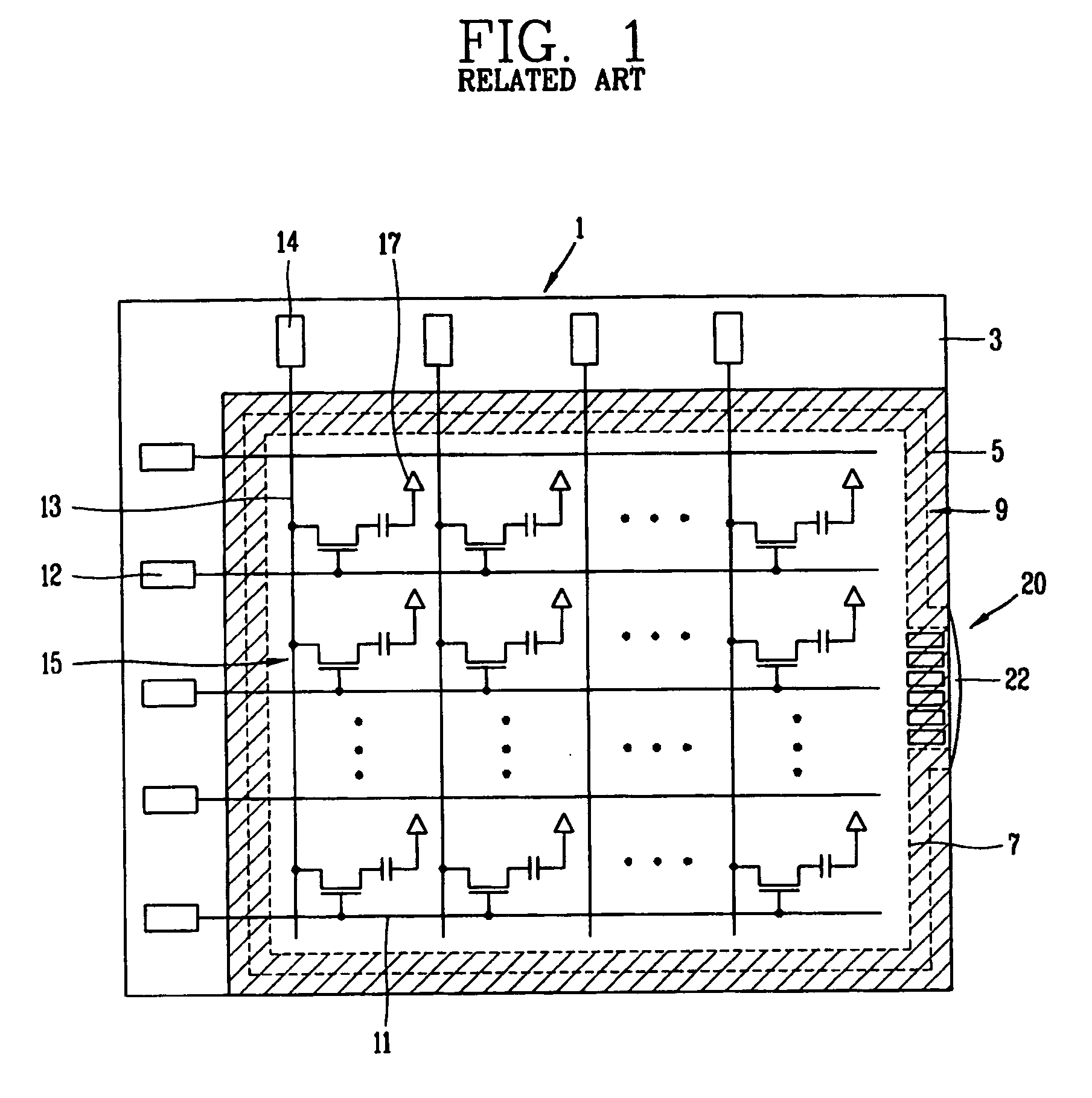
[0040]In a liquid crystal display device using an inorganic material as a passivation layer, because a pixel electrode is formed on the inorganic passivation layer, it is required to maintain a gap between a gate line (for applying a scan signal from the outside to a gate electrode) and a pixel electrode or between a data line (for applying an image signal from the outside to a source / drain electrode) and the pixel electrode. If the gate line or the data line overlaps a part of the pixel electrode having the passivation layer therebetween, a parasitic capacitance occurs, and accordingly vertical crosstalk occurs. The crosstalk causes a flicker phenomenon, and it is a major cause for reducing a picture qual...


PUM

PropertyMeasurementUnit
widthsaaaaaaaaaa
light transmissionaaaaaaaaaa
slit widthaaaaaaaaaa

Abstract

A method of fabricating a liquid crystal display device is disclosed in the present invention. The method includes forming a thin film transistor in a pixel region and a pad on an edge region of a first substrate, depositing an organic passivation layer over the first substrate, and removing the organic passivation layer in the edge region using a diffraction mask to expose a portion of the pad, wherein the diffraction mask has a slit portion including a plurality of slits having different widths.

Description

[0001]This application claims the benefit of the Korean Patent Application No. P2002-087480 filed on Dec. 30, 2002, which is hereby incorporated by reference.BACKGROUND OF THE INVENTION[0002]1. Field of the Invention[0003]The present invention relates to a liquid crystal display device, and more particularly, to a method of fabricating a liquid crystal display device. Although the present invention is suitable for a wide scope of applications, it is particularly suitable for removing a hangover of an organic insulating layer around an edge portion of a pad by using a diffraction mask.[0004]2. Discussion of the Related Art[0005]A liquid crystal display device as a transmissive flat display device is widely applied to various electronic equipments, such as mobile phones, personal digital assistants (PDA's), and notebook computers. Recently, the LCD has been in the spotlight due to its advantages, such as light weight, slim shape, and high definition reproducibility. Furthermore, accor...

Claims


Application Information

Patent Timeline
Patent Type & Authority Patents(United States)
IPC IPC(8): H01L21/00G02F1/1339H01L29/10G02F1/13G02F1/1362
CPCG02F1/13458G02F1/136227G02F2001/136236G02F1/136236G02F1/13
Inventor SONG, IN-DUKRYU, HO-JIN
Owner LG DISPLAY CO LTD
Why Eureka
Try Eureka