Scintillation materials with reduced afterglow and method of preparation

a technology of scintillation materials and afterglow, applied in the field of scintillation materials, can solve the problems of significant material loss during processing, ceramic gos, even more expensive, and the cost and availability of scintillation materials and any necessary machining,

Active Publication Date: 2007-02-20
ALEXANDER LEMPICKI
View PDF17 Cites 43 Cited by
  • Summary
  • Abstract
  • Description
  • Claims
  • Application Information

AI Technical Summary

Problems solved by technology

Commercial applications such as CT require a very large number of scintillator elements, so that the cost and availability of the scintillation material and any necessary machining have become very important issues.
Another new exotic material, which is now being used in CT systems, is ceramic GOS, which is even more expensive.
Moreover, the machining of CdWO4 pixels to dimensions as small as 0.8×0.8 mm becomes particularly expensive process due to the brittle nature of the crystal, resulting in significant material loss during processing.
Due to the limitations in the availability of x-ray flux, all such applications require a scintillator with very high x-ray absorption and high light output.
This causes pulse pileup in high count rate applications, reconstruction artifacts in CT applications, and problems of reduced contrast and image blurring in high speed x-ray imaging.
Its companion alkali halide scintillators, KI(Tl) and KCl(Tl), have played a very important role in our understanding of scintillator phenomena but have not been considered as viable scintillators for practical use.
Pure (undoped) NaI is not a good scintillator, emitting only poorly at room temperature.
All are strongly temperature quenched, making the decay time progressively shorter and reducing the efficiency of both radiative and excitonic transfer in most of these materials.
However, since concentration quenching typically limits the Tl doping level to about the 1000-ppm range in CsI(Tl), very few of these charge carriers are formed close enough to the Tl ions to excite them directly.
A serious problem in all alkali halides is that the mobility of carriers is very small due to self-trapping.
This is a primary reason for the complexity of the scintillation process in the alkali halides.
Such VK centers in CsI(Tl), created by prolonged x-irradiation at low temperature, were investigated by the technique of magnetic circular dichroism of absorption (MCDA), from which it was concluded that the Tl+ ions serve as shallow hole traps, and consequently that persistent afterglow is unavoidable in this material.

Method used


Image

  • Scintillation materials with reduced afterglow and method of preparation
  • Scintillation materials with reduced afterglow and method of preparation
  • Scintillation materials with reduced afterglow and method of preparation

Examples


Embodiment Construction

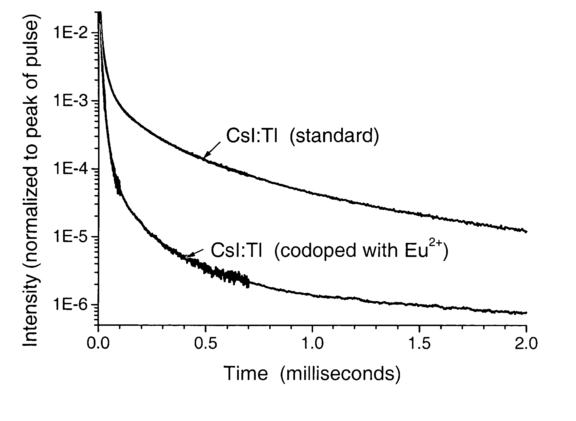
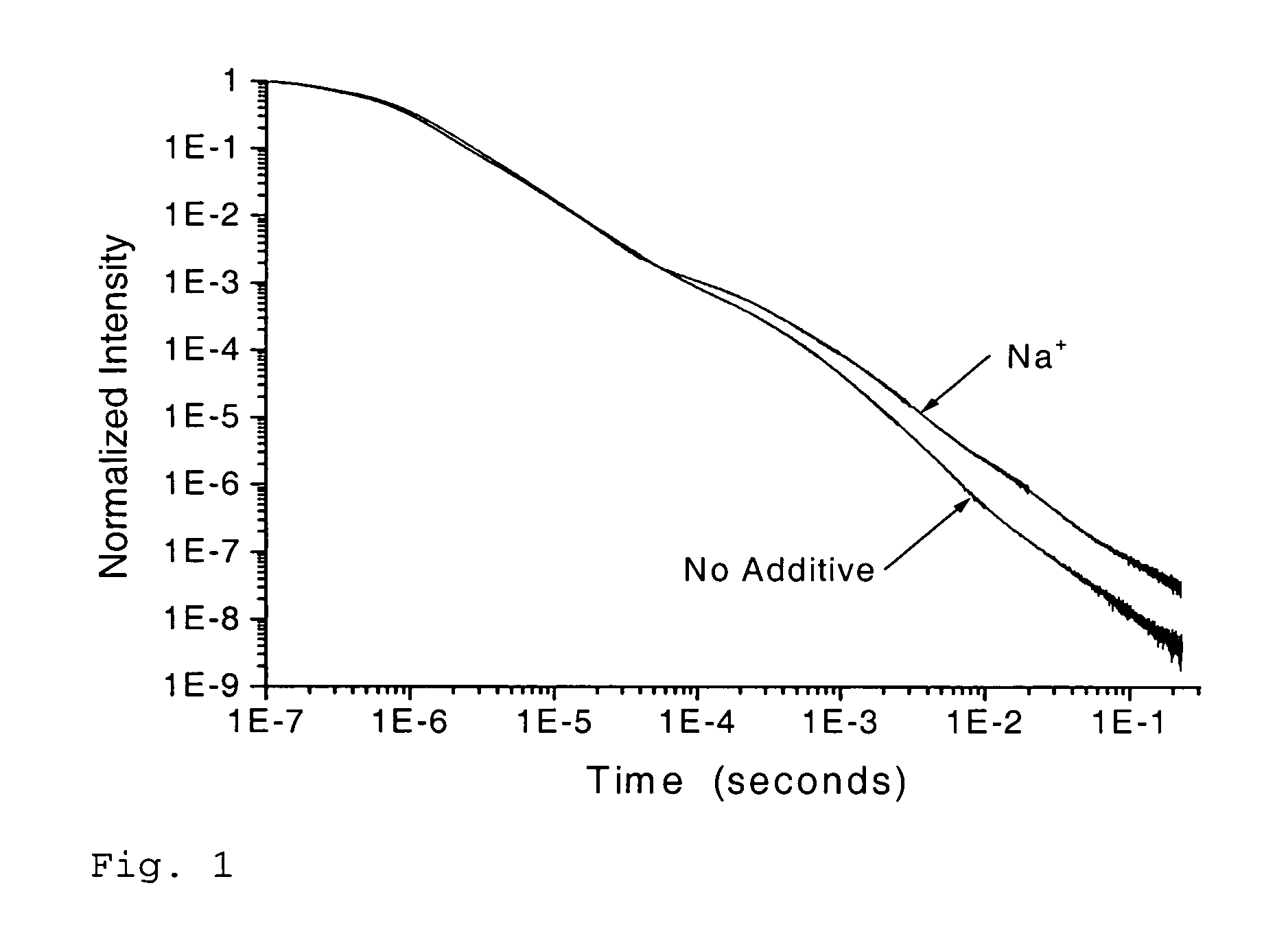
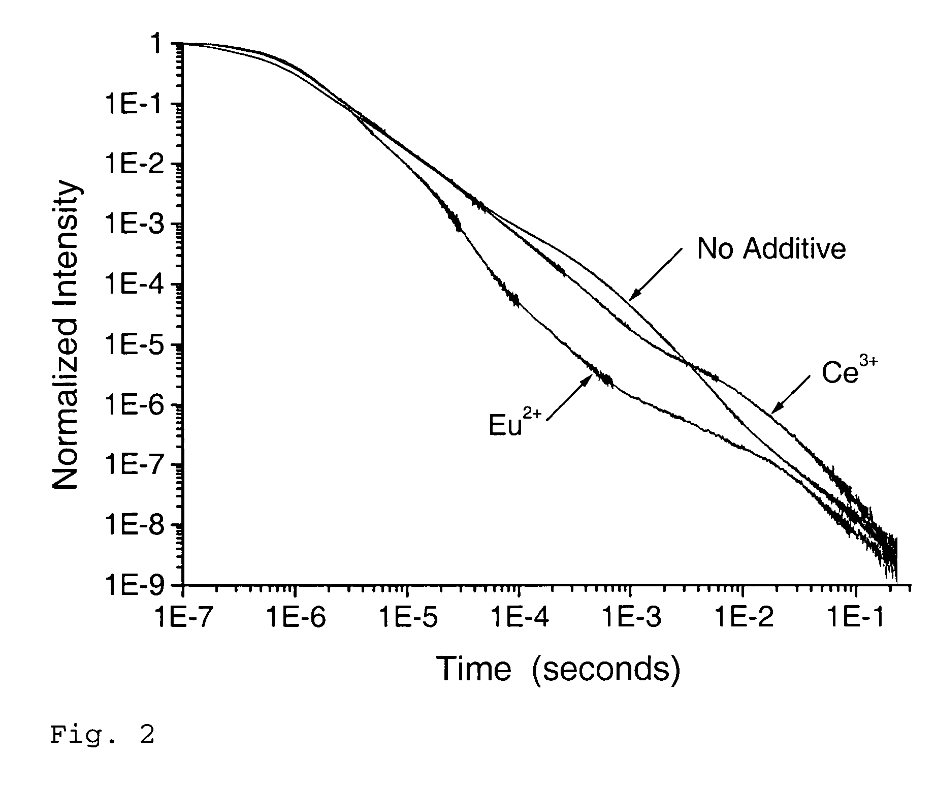
[0041]Scintillation materials with reduced residual afterglow, methods to fabricate scintillation materials with reduced residual afterglow, where the scintillation materials have either single crystal or multiple columnar structure, and systems utilizing the materials of this invention are described hereinbelow.

[0042]In one embodiment, scintillation materials of this invention have an alkali halide host material, a (first) scintillation dopant of various types, and a variety of second dopants (co-dopants). In another embodiment, scintillation materials of this invention have an alkali halide host material, a (first) scintillation dopant of various types, a variety of second dopants (co-dopants), and a variety of third dopants (co-dopants). The co-dopants of this invention are selected to divert carriers away from the sources of the afterglow and recycle them rapidly enough to enhance the desired prompt emission.

[0043]The level of scintillation doping (activator concentration) requi...


PUM


Abstract

Scintillation materials of this invention have an alkali halide host material, a (first) scintillation dopant of various types, and a variety of second dopants (co-dopants). In another embodiment, the scintillation materials of this invention have an alkali halide host material, a (first) scintillation dopant of various types, a variety of second dopants (co-dopants), and a variety of third dopants (co-dopants). Co-dopants of this invention are capable of providing a second auxiliary luminescent cation dopant, capable of introducing an anion size and electronegativity mismatch, capable of introducing a mismatch of anion charge, or introducing a mismatch of cation charge in the host material.

Description

STATEMENT OF GOVERNMENT INTEREST[0001]This invention was made partially with U.S. Government support from the National Institutes of Health (NIH) under contract no. 1R43CA92806-1 (also referred to as CA92806). The U.S. Government has certain rights in the invention.BACKGROUND OF THE INVENTION[0002]This invention relates generally to scintillation materials, and, more particularly, to scintillation materials with reduced afterglow.[0003]Scintillation detectors are used in a wide variety of applications ranging from medical imaging to high-energy physics (HEP). The development of new scintillators with better properties, complemented by advances in silicon based readout technologies such as high-gain avalanche photodiodes (APDs), have significantly advanced the present detector state-of-the-art. High resolution x-ray detectors based on amorphous silicon sensor arrays (a-Si:H) or charge coupled devices (CCD) in conjunction with scintillator films have been developed, and are now routin...

Claims


Application Information

Patent Timeline
Patent Type & Authority Patents(United States)
IPC IPC(8): G01T1/00
CPCC09K11/772C09K11/7733G21K4/00G01T1/2023G21K2004/06
Inventor BRECHER, CHARLESNAGARKAR, VIVEK
Owner ALEXANDER LEMPICKI
Why Eureka
Try Eureka