Supercharge Your Innovation With Domain-Expert AI Agents!

Circuit and method for storing data in operational and sleep modes

a technology of circuits and circuits, applied in the field of data processing systems, can solve the problems of balloon latches consuming considerable additional circuit area, limited design, loss of state within circuitry,

Active Publication Date: 2007-02-20
ARM LTD
View PDF8 Cites 27 Cited by
  • Summary
  • Abstract
  • Description
  • Claims
  • Application Information

AI Technical Summary

Benefits of technology

This approach effectively retains data during sleep mode with minimal additional circuitry and control signals, reducing power leakage and consumption while allowing for efficient power management.

Problems solved by technology

To enter a low leakage mode, the power transistors are turned off and the leakage of the design is limited by the leakage of the power transistors.
Although this results in substantial power savings it also results in a loss of state within the circuitry.
A disadvantage of this approach is that the balloon latches consume considerable additional circuit area.
Whilst this approach reduces the increase in circuit overhead associated with providing the data retention capability, it does require control of the three clock signals of the sense amplifier flip-flops or hybrid latch flip-flops with their known disadvantages in terms of speed, power consumption and other factors.

Method used


Image

  • Circuit and method for storing data in operational and sleep modes
  • Circuit and method for storing data in operational and sleep modes
  • Circuit and method for storing data in operational and sleep modes

Examples


Embodiment Construction

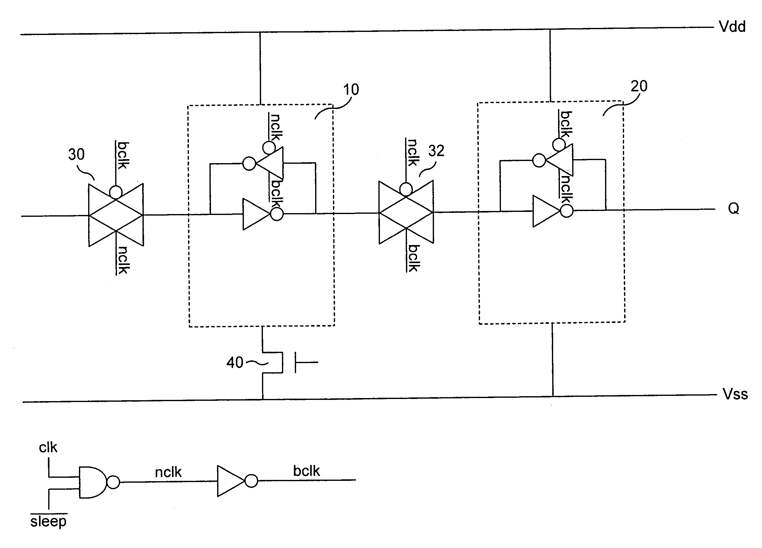
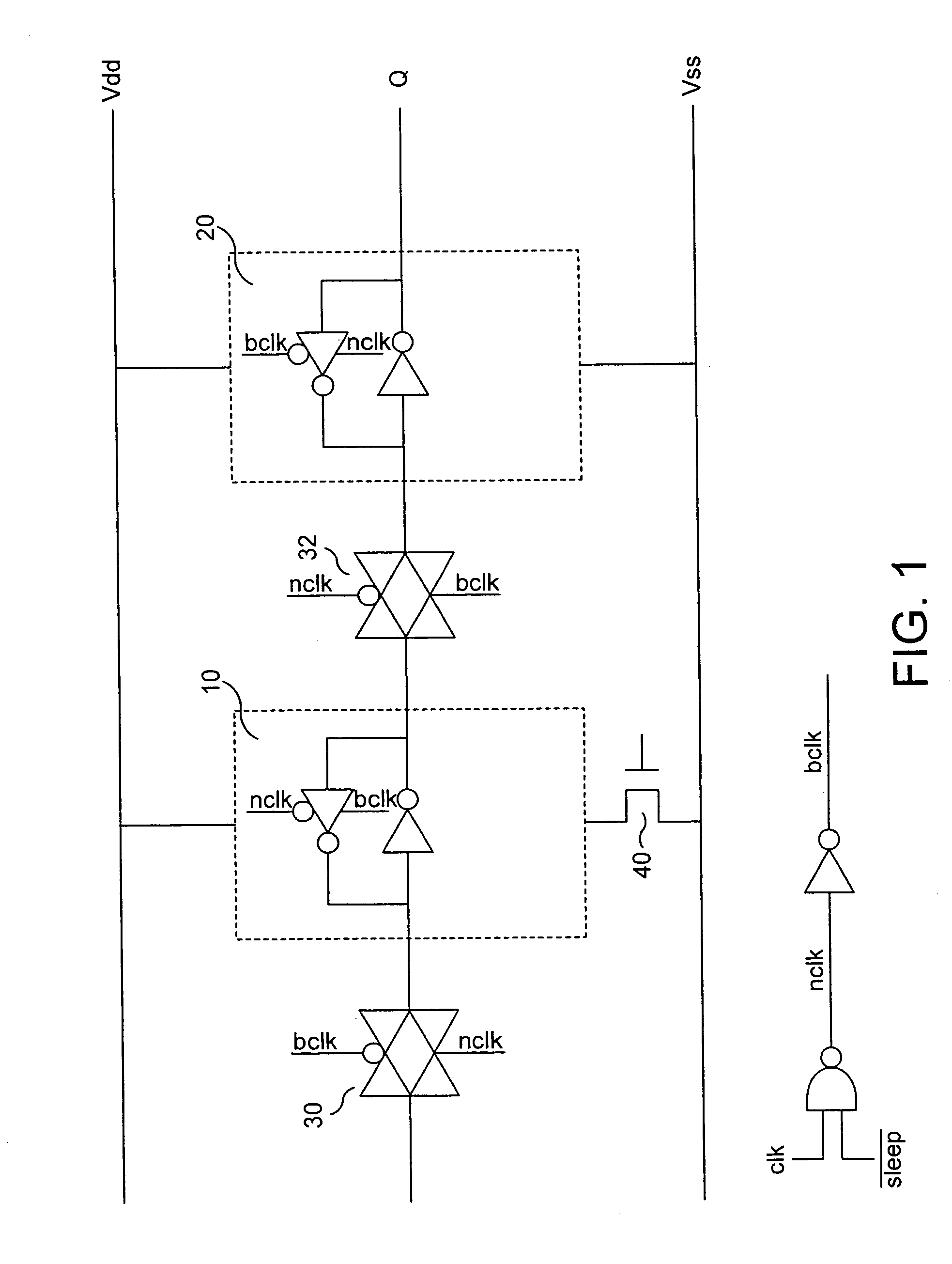
[0046]The circuit of FIG. 1 shows a circuit that is operable to retain state during sleep mode according to an embodiment of the present invention. The circuit comprises two latches 10, 20 arranged in series and each having a tristateable device 30, 32 at its input. The tristateable devices 30, 32 are, in this embodiment, transmission gates, although other tristateable devices could be used, such as a tristate inverter or tristateable logic.

[0047]In the device shown latch 10, the master latch in this embodiment, comprises a power transistor 40 between it and the lower voltage rail Vss. This means that in response to a sleep signal at the gate of the power transistor 40, power transistor 40 turns off and the output of the power transitor floats towards Vdd, thus the voltage drop across latch 10 reduces and latch 10 is powered down and will lose state.

[0048]Slave latch 20 is not connected to Vss via the power transistor and thus, it will not be powered down by the sleep signal and it ...


PUM


Abstract

The application relates to a circuit for storing a signal during sleep mode, said embodiments of the circuit comprising: a sleep signal input operable to receive a sleep signal; a clock signal input operable to receive a clock signal; a plurality of latches clocked by said clock signal, at least one tristateable device clocked by said clock signal, said at least one tristateable device being arranged at an input of at least one of said plurality of latches, said at least one tristateable device being operable to selectively isolate said input of said at least one latch in response to a predetermined clock signal value; clock signal distribution means operable to distribute said clock signal to said plurality of latches and said at least one tristateable device; wherein in response to a sleep signal said circuit is operable to: reduce a voltage difference across at least a portion of said circuit such that said portion of said circuit is powered down; and maintain a voltage difference across at least one storage latch, said at least one storage latch being said at least one of said plurality of latches; said clock signal distribution means being operable to hold said clock signal at said predetermined value such that said input of said storage latch is isolated.

Description

BACKGROUND OF THE INVENTION[0001]1. Field of the Invention[0002]This invention relates to the field of data processing systems. More particularly, this invention relates to circuits and methods of operating circuits which allow for the storage of a signal value in operational and sleep modes.[0003]2. Description of the Prior Art[0004]In many circuits, particularly those that run off remote power supplies such as batteries, it is important to keep the power consumption of the circuits low. As well as addressing the issue of operational circuit efficiency attention is also being turned to reducing static power loss, i.e. power loss due to power leakage occurring while a circuit is not performing operations. One way of addressing this is to provide the circuit with a sleep mode so that it is in effect powered down during these non-operational periods. To reduce power leakage during these sleep periods, many circuit designs are now making use of power gating which helps make the sleep m...

Claims


Application Information

Patent Timeline
Patent Type & Authority Patents(United States)
IPC IPC(8): H03K3/12
CPCG06F1/3203G06F1/3237G06F1/3296H03K3/0375H03K3/0372H03K3/012Y02B60/32Y02B60/1221Y02B60/1285Y02D10/00Y02D30/50G06F1/32H03K19/00H03K3/12H03K3/00
Inventor FREDERICK, MARLINKINKADE, MARTIN JAY
Owner ARM LTD
Features
  • R&D
  • Intellectual Property
  • Life Sciences
  • Materials
  • Tech Scout
  • Unparalleled Data Quality
  • Higher Quality Content
  • 60% Fewer Hallucinations
Learn More