Waveguide type optical device using large third order non-linearity optical material and method for operating the same

a waveguide and optical material technology, applied in the field of waveguide-type optical devices, can solve the problems of poor industrial utility, deterioration of device performance, and inability to integrate devices, and achieve the effect of minimizing the loss of a signal beam, efficient operation and easy manufacturing processes

Active Publication Date: 2007-02-20
KOREA INST OF SCI & TECH
View PDF7 Cites 34 Cited by
  • Summary
  • Abstract
  • Description
  • Claims
  • Application Information

AI Technical Summary

Benefits of technology

[0024]Another object of the present invention is to provide a waveguide type optical device in which interfacial ununiformity between different kinds of materials in a waveguide is prevented from occurring.
[0025]Another object of the present invention is to provide a unit device for all-optical communications, such as an optical switch and an optical modulator for an integrated optical device which can be manufactured through easy manufacturing processes and can be efficiently operated by minimizing a loss of a signal beam.

Problems solved by technology

This type of 3rd order nonlinear optical effect has advantages such as less light absorption, fast response time, but it also has disadvantages of very small 3rd order nonlinear optical coefficient value.
However, such devices are impossible to be integrated because of its long waveguide.
Also, the devices are very sensitive to temperature change, which deteriorates device performance, and thus have poor industrial utility.
However, this type is disadvantageous in that light cannot be guided in a long distance because linear absorption of light in a material is great, and that its response time is slower compared to the non-resonance type.
This composite material is disadvantageous in that an operation speed is limited to tens of pico seconds at best because it requires interband transition of a real charge carrier, but is advantageous in that a 3rd order nonlinear susceptibility is large and its operation wavelength (band) can be tailored within a relatively large wavelength range only by changing its particle size.
This type of composite material has somewhat restrictive in changing operation wavelength compared to the composite materials made by dispersing semiconductor particles.
Also, the nano-composite material using metal nano-particles disadvantageously has large absorption of light in the wavelength region of surface plasmon resonance in which 3rd order nonlinear optical effect is maximized.
The absorption makes actual embodiment of a waveguide type optical device very difficult.
On the contrary, if the phases of two beams are opposite at the moment of the interference, thereby causing a destructive interference, no light is outputted from the output port 2f.
If there is a pump beam causing a 3rd order nonlinear optical phenomenon, destructive interference of the signal beam occurs at the output port 2f of the waveguide, thereby outputting no signal beam.
However, its manufacturing is practically difficult since the waveguide should include a 3rd order nonlinear optical material part 3 therein.
However, matching the refractive indices is very difficult.
Furthermore, even though the refractive index matching is realized, it is almost impossible to remove interfacial loss in a manufacturing process.
Accordingly, it is very difficult to implement the 3rd order nonlinear optical switching device shown in FIG. 2.

Method used


Image

  • Waveguide type optical device using large third order non-linearity optical material and method for operating the same
  • Waveguide type optical device using large third order non-linearity optical material and method for operating the same
  • Waveguide type optical device using large third order non-linearity optical material and method for operating the same

Examples


Embodiment Construction

[0045]Reference will now be made in detail to the preferred embodiments of the present invention, examples of which are illustrated in the accompanying drawings.

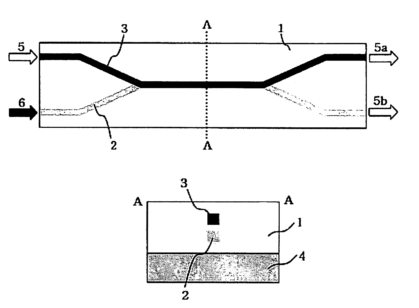
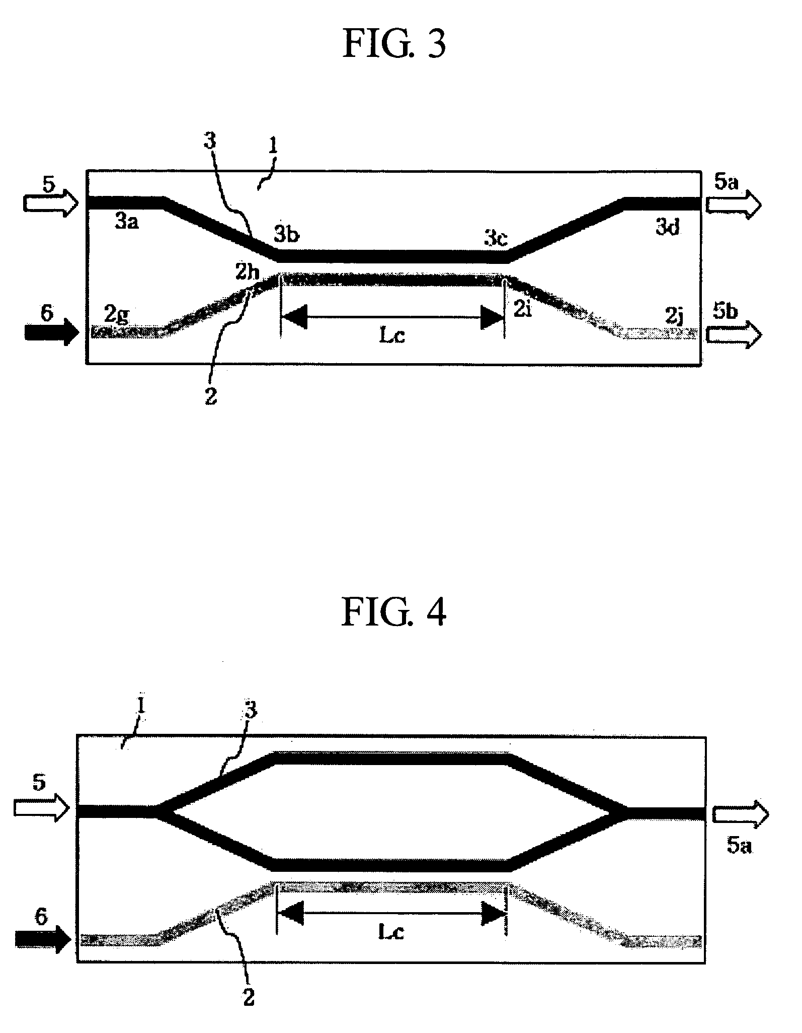
[0046]FIG. 3 is a plan view showing a basic concept of a waveguide type optical device in accordance with the present invention, and is a view showing a waveguide type optical device in a form of directional coupler. As shown in FIG. 3, the waveguide type optical device in a form of directional coupler includes an upper signal beam waveguide 3 and a lower pump beam waveguide 2. In the upper signal beam waveguide 3 formed of a 3rd order nonlinear optical material which absorbs no light in a signal beam wavelength, a pump beam having a wavelength of a surface plasmon resonance cannot be guided due to a large linear absorption coefficient, and a signal beam having a wavelength at which little absorption is made by the material is guided. Meanwhile, the entire lower pump beam waveguide 2 is formed of a material which absorbs a v...


PUM

PropertyMeasurementUnit
wavelengthaaaaaaaaaa
surface plasmon resonance wavelengthaaaaaaaaaa
refractive indexaaaaaaaaaa

Abstract

Disclosed is a waveguide type optical device utilizing a nonlinear refractive index change according to a large 3rd order nonlinear optical phenomenon. The waveguide type optical device includes a signal beam waveguide through which a signal beam propagates; and a pump beam waveguide through which a pump beam propagates, wherein the pump beam waveguide is disposed adjacent to the signal beam waveguide so that the pump beam can be coupled to the signal beam waveguide, the signal beam waveguide is made of nonlinear optical materials with large 3rd order nonlinear optical property and the pump beam waveguide is made of linear optical materials, and the wavelength range of the signal beam is different from that of the pump beam. By such a structure, the pump beam is coupled to one arm of the signal beam waveguide, thereby generating a 3rd nonlinear phenomenon on one arm of the waveguide through which the signal beam passes. Therefore, the waveguide optical device which implements an all-optical communication device operating as an optical device and can be integrated is provided.

Description

BACKGROUND OF THE INVENTION[0001]1. Field of the Invention[0002]The present invention relates to a waveguide type optical device, and particularly, to an optical device using 3rd order nonlinear optical material.[0003]2. Description of the Background Art[0004]In order to implement an all-optical device such as optical switches and optical modulators for data processing at higher speed, nonlinear refractive index change, one of 3rd order nonlinear optical effects, can be used. In the phenomenon, refractive index of a medium is changed due to change of incident light intensity.[0005]The 3rd order nonlinear optical effect in a medium can be classified into two kinds depending on its generation mechanism. In one of them, 3rd order nonlinear optical effect is achieved in a state that laser beam incident on an optical material is little absorbed. In this type, not resonance such as excitation of a material due to light absorption, but ‘non-resonance effect’, such as optical Kerr effect in...

Claims


Application Information

Patent Timeline
Patent Type & Authority Patents(United States)
IPC IPC(8): G02B6/26G02B6/12G02F1/35
CPCG02F1/3517G02B2006/12142G02B2006/12145G02F1/3521G02B2006/12147G02B6/12
Inventor LEE, TAEK-SUNGLEE, KYEONG SEOKKIM, WON-MOKCHEONG, BYUNG-KIKIM, IN-HO
Owner KOREA INST OF SCI & TECH
Why Eureka
Try Eureka