Method of forming silicon-on-insulator (SOI) semiconductor substrate and SOI semiconductor substrate formed thereby

a technology of silicon-on-insulator and semiconductor substrate, which is applied in the direction of semiconductor devices, electrical appliances, basic electric elements, etc., can solve problems such as current leakage and become a serious problem

Inactive Publication Date: 2007-02-27
SAMSUNG ELECTRONICS CO LTD
View PDF16 Cites 205 Cited by
  • Summary
  • Abstract
  • Description
  • Claims
  • Application Information

AI Technical Summary

Benefits of technology

[0008]A feature of the present invention is to provide a method of forming an SOI semiconductor substrate that prevents impurities implanted into an SOI layer from being diffused into a buried oxide layer and a semiconductor substrate, and the SOI semiconductor substrate formed thereby.

Problems solved by technology

For this reason, current leakage, current leaked into the semiconductor substrate through the source / drain region, can become a serious problem.

Method used


Image

  • Method of forming silicon-on-insulator (SOI) semiconductor substrate and SOI semiconductor substrate formed thereby
  • Method of forming silicon-on-insulator (SOI) semiconductor substrate and SOI semiconductor substrate formed thereby
  • Method of forming silicon-on-insulator (SOI) semiconductor substrate and SOI semiconductor substrate formed thereby

Examples


Embodiment Construction

[0022]The present invention will now be described more fully hereinafter with reference to the accompanying drawings, in which preferred embodiments of the invention are shown. The invention may, however, be embodied in different forms and should not be construed as limited to the embodiments set forth herein. Rather, these embodiments are provided so that this disclosure will be thorough and complete, and will fully convey the scope of the invention to those skilled in the art. In the drawings, the thickness of layers and regions are exaggerated for clarity. It will also be understood that when a layer is referred to as being “on” another layer or substrate, it can be directly on the other layer or substrate, or intervening layers may also be present. Like numbers refer to like elements throughout.

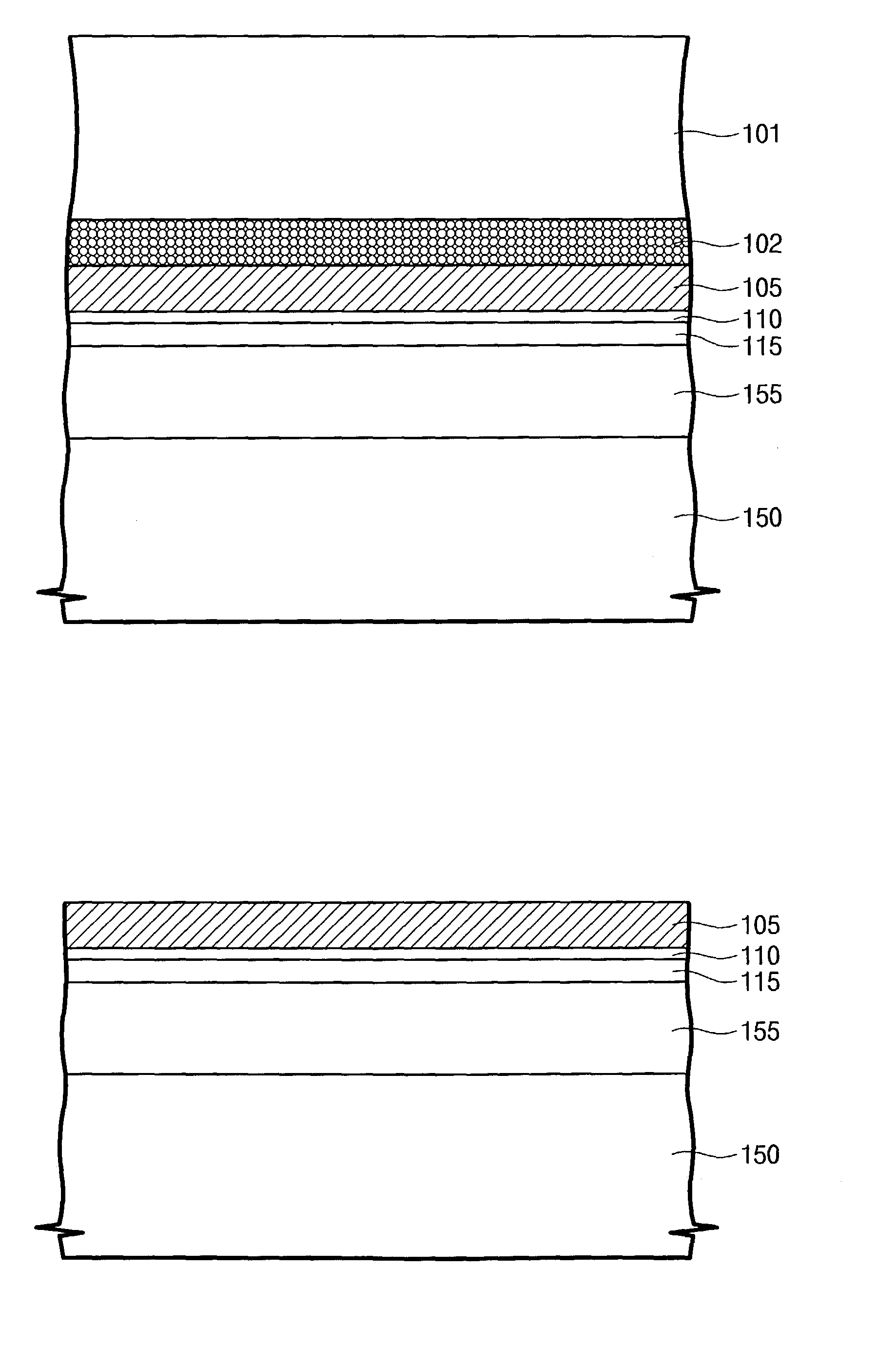
[0023]FIGS. 3 through 6 are cross-sectional views showing a method of forming an SOI semiconductor substrate according to a preferred embodiment of the present invention.

[0024]Referring t...


PUM


Abstract

A method of forming an SOI semiconductor substrate and the SOI semiconductor substrate formed thereby, is provided. The method includes forming sequentially buried oxide, diffusion barrier and SOI layers on a semiconductor substrate. The diffusion barrier layer is formed by an insulating layer having a lower impurity diffusion coefficient as compared with the buried oxide layer. The diffusion barrier layer serves to prevent impurities implanted into the SOI layer from being diffused into the buried oxide layer or the semiconductor substrate.

Description

FIELD OF THE INVENTION[0001]The present invention relates to a method of forming a semiconductor device and the semiconductor device formed thereby; more particularly, a method of forming an SOI semiconductor substrate and the SOI semiconductor substrate formed thereby.BACKGROUND OF THE INVENTION[0002]A typical transistor has a source / drain region, which is defined by forming an impurity diffusion layer at a semiconductor substrate. A PN junction is formed between the source / drain region and the semiconductor substrate. Accordingly, the semiconductor substrate and the source / drain region are electrically isolated from each other when a reverse bias is applied therebetween.[0003]With trends toward higher integration of semiconductor devices, a depth of the source / drain region is continually reduced. For this reason, current leakage, current leaked into the semiconductor substrate through the source / drain region, can become a serious problem. One proposed solution to suppress the curr...

Claims


Application Information

Patent Timeline
Patent Type & Authority Patents(United States)
IPC IPC(8): H01L21/76H01L21/02H01L21/762H01L27/12
CPCH01L21/76259H01L21/76254H01L27/12
Inventor LEE, JUNG-ILBAE, GEUM-JONGKIM, KI-CHULRHEE, HWA-SUNGKIM, SANG-SU
Owner SAMSUNG ELECTRONICS CO LTD
Why Eureka
Try Eureka