Sampling switch

a sampling switch and switch technology, applied in the field of sampling switches, can solve the problems of large distortion added to the signal, the voltage at the source terminal and the drain terminal cannot be considered to change in the same fashion when the input signal changes in high speed, and the conversion characteristics of the a/d converter will be impaired, so as to improve the accuracy of analog signal processing and reduce the distortion of the signal

Inactive Publication Date: 2007-02-27
FUJITSU LTD
View PDF5 Cites 32 Cited by
  • Summary
  • Abstract
  • Description
  • Claims
  • Application Information

AI Technical Summary

Benefits of technology

[0022]In consideration of the above described problems, an object of the present invention is to control a voltage between the gate and source so as to apply an input voltage by a delayed time according to the delay time of the output voltage from an input voltage and, at the same time, so as to maintain a voltage between the substrate and source constant at approximately zero volt, or independently control a delay of voltage between the gate and source, and a delay of voltage between the substrate and source, thereby reducing a distortion of the signal induced by changes in the on-resistance of a sampling switch and improving the accuracy of analog signal processing.

Problems solved by technology

For example, if a signal wave form is deformed by a sampling switch sampling an analog signal in an A / D converter, that is, if the wave form of the input signal is changed from that of an input signal, the conversion characteristics of the A / D converter will be impaired.
In the second example of a conventional technique, however, since the output signal outputted from the drain terminal of the transistor 100 is delayed relative to the input signal, voltages at the source terminal and the drain terminal cannot necessarily be considered to change in the same fashion when the input signals change in high speeds.
Therefore, although it may be considered that maintaining the gate terminal voltage constant in accordance with the average between the source and drain terminal voltages should suppress a variation of the on-resistance of a transistor to a small value, keeping the voltage between the gate and source unilaterally allows the voltage between the gate and drain to fluctuate in great deal as indicated in the second example of a conventional technique shown by FIG. 2, thus leaving a problem of causing a large distortion added to the signal unresolved.
In the meantime, while the on-resistance of a transistor depends on the voltage between the substrate and the source, the problem of reducing a distortion cannot be accomplished by this control because the substrate voltage is actually considered to be maintained at a fixed potential in the second example of a conventional technique shown in FIG. 2.
Such a conventional technique of controlling the gate voltage by using a bootstrap circuit is described in a patent document below, the technique of which has not solved the same problem as with the second example of a conventional technique, however.
However, as for controlling a voltage between the substrate and source, a substrate terminal voltage control is performed only by the output signal voltage, leaving the unsolved problem of a small effect on reducing a distortion of signal as compared to a control by the intermediate voltage between the input signal and output signal voltages.
Furthermore, the third example of a conventional technique requires the same circuitry of control circuit on both side of the transistor 100, i.e., the fundamental switch, causing a problem of larger circuit area.

Method used


Image

  • Sampling switch
  • Sampling switch
  • Sampling switch

Examples


first embodiment

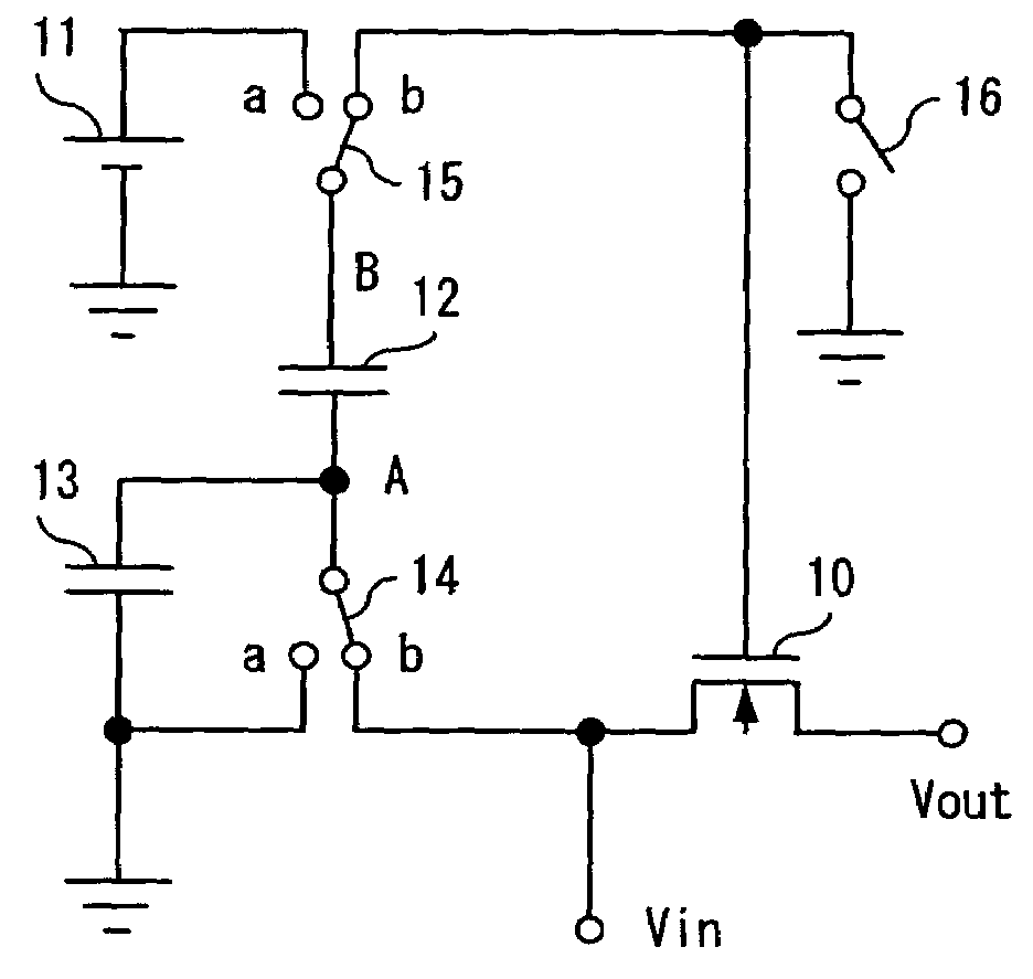
[0048]FIG. 5 shows a basic circuit configuration of a sampling switch according to the present invention. In FIG. 5, the sampling switch comprises a MOS transistor 10 for being applied by an input voltage Vin to the source terminal thereof and outputting an output voltage Vout from the drain terminal thereof, a supply source 11, capacitances 12 and 13, and switches 14, 15 and 16. These elements except for the MOS transistor 10 constitute a gate voltage control unit noted in claims of the present invention.

[0049]The first embodiment is an embodiment enabling a control circuit comprising a bootstrap circuit for controlling a gate terminal voltage of the MOS transistor 10 to control a delay time of the gate terminal voltage relative to an input voltage Vin in accordance with a delay time of the output voltage Vout relative to the input voltage Vin.

[0050]In FIG. 5, when the input voltage Vin is applied to the source terminal, the MOS transistor 10 is not in conduction, i.e., turned off,...

second embodiment

[0055]In the second embodiment shown by FIG. 6, a voltage between the substrate and source is maintained constant at approximately zero volt by the switch 14 actually connecting the substrate and source terminals of the MOS transistor 10. This enables the voltage between the substrate and source to be maintained approximately constant, in addition to the voltage between the gate and source and that across the gate and drain in the state of the sampling switch being in conduction, thereby further decreasing a change in the on-resistance of the transistor and therefore a distortion of signals induced by the sampling switch.

[0056]While the same effect is gained for the gate terminal voltage control of the MOS transistor 10 as the first embodiment shown by FIG. 5, a capacitance value of the capacitance 13 must be controlled at a smaller value in comprehension of a parasitic capacitance of the substrate terminal since the substrate terminal of the transistor 10 is connected to the node A...

third embodiment

[0079]In the third embodiment shown by FIG. 13, the transistor 35 corresponds to the terminal “b” of the switch 17, the transistor 36 corresponds to the terminal “a” thereof, and the capacitance 37 corresponds to the capacitance 18, each corresponded element respectively shown by FIG. 7. By this configuration, during a time of the transistor 10 being turned off, the transistor 35 is turned on and the substrates of transistors 10 and 35 are both at the ground potential Vss.

[0080]Contrarily, during a time of the transistor 10 being turned on, the transistor 35 is turned on, and the transistor 10 is applied, as the substrate terminal voltage thereof, by an input voltage Vin with a delay time according to a time constant determined by the on-resistance of the transistor 35 and the capacitance of node-C, i.e., the sum of the parasitic capacitance of the node-C and the capacitance of the capacitance 37.

[0081]FIG. 14 shows an example of a sample hold circuit as an exemplified embodiment of...


PUM


Abstract

A sampling switch is the one for sampling an input voltage and providing an output voltage, comprising a MOS transistor for being supplied by the input voltage to the source terminal thereof and providing the output voltage from the drain terminal thereof; and a gate voltage control unit for supplying a voltage to the gate terminal of the MOS transistor with a delayed time from the input voltage. This enables a change in the on-resistance of a MOS transistor used for a sampling switch to be suppressed to a minimum, thereby reducing a distortion of signals induced by a change in the on-resistance.

Description

CROSS-REFERENCE TO RELATED APPLICATIONS[0001]This application is based upon and claims the benefit of priority from the prior Japanese Patent Application No.2004-150571, filed in May, 20, 2004, the entire contents of which are incorporated herein by reference.BACKGROUND OF THE INVENTION[0002]1. Field of the Invention[0003]The present invention relates to a sampling switch used for an analog signal processing, specifically to a sampling switch capable of reducing a distortion in a signal wave form caused by a variation of on-resistance thereof being unaffected by a fluctuation of the input voltage thereto.[0004]2. Description of the Related Art[0005]Sampling switches are widely used for the analog signal processing such as a sample hold circuit, a switched capacitor circuit and an analog-to-digital (“A / D” hereinafter) converter. An important property of such a switch used in the signal path for an analog signal is that the on-resistance thereof does not cause a distortion in the sign...

Claims


Application Information

Patent Timeline
Patent Type & Authority Patents(United States)
IPC IPC(8): G11C27/02H03K5/00H03K17/06H03K17/00H03K17/16H03K17/687
CPCH03K17/063G11C27/02H03K17/00H03K17/16
Inventor KUDO, MASAHIRO
Owner FUJITSU LTD
Why Eureka
Try Eureka