Semiconductor optical device

a semiconductor and optical device technology, applied in the direction of optical elements, semiconductor lasers, instruments, etc., can solve the problems of significant backscattering of light and adversely affect the operation of optical components, and achieve the effect of efficiently modulating substantially the entire optical mode and avoiding the consequences of etching through the active layer of the laser

Active Publication Date: 2007-02-27
LUMENTUM TECH UK LTD
View PDF13 Cites 36 Cited by
  • Summary
  • Abstract
  • Description
  • Claims
  • Application Information

AI Technical Summary

Benefits of technology

[0006]The present invention seeks to provide semiconductor optical devices in which a transition between a ridge waveguide having a relatively low ridge (e.g. a shallowly etched ridge) and a ridge waveguide having a relatively high ridge (e.g. deeply etched ridge) causes minimal back-scattering (e.g. reflection) of light. The suppression of back-scattering is often important, because back-scattered light can adversely affect the operation of optical components (e.g. lasers). A transition between a relatively low ridge, and a relatively high ridge, of a ridge waveguide can cause significant back-scattering of light. However, it can be advantageous to have ridge waveguides with different height ridges (i.e. ridges etched to different depths) fabricated on one and the same semiconductor optical device, because the heights of the ridges can be tailored to the needs of different optical components integrat

Problems solved by technology

The suppression of back-scattering is often important, because back-scattered light can adversely affect the operation of optical components (e.g. l

Method used


Image

  • Semiconductor optical device
  • Semiconductor optical device
  • Semiconductor optical device

Examples


Embodiment Construction

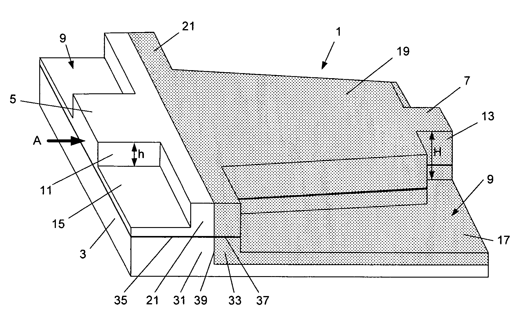
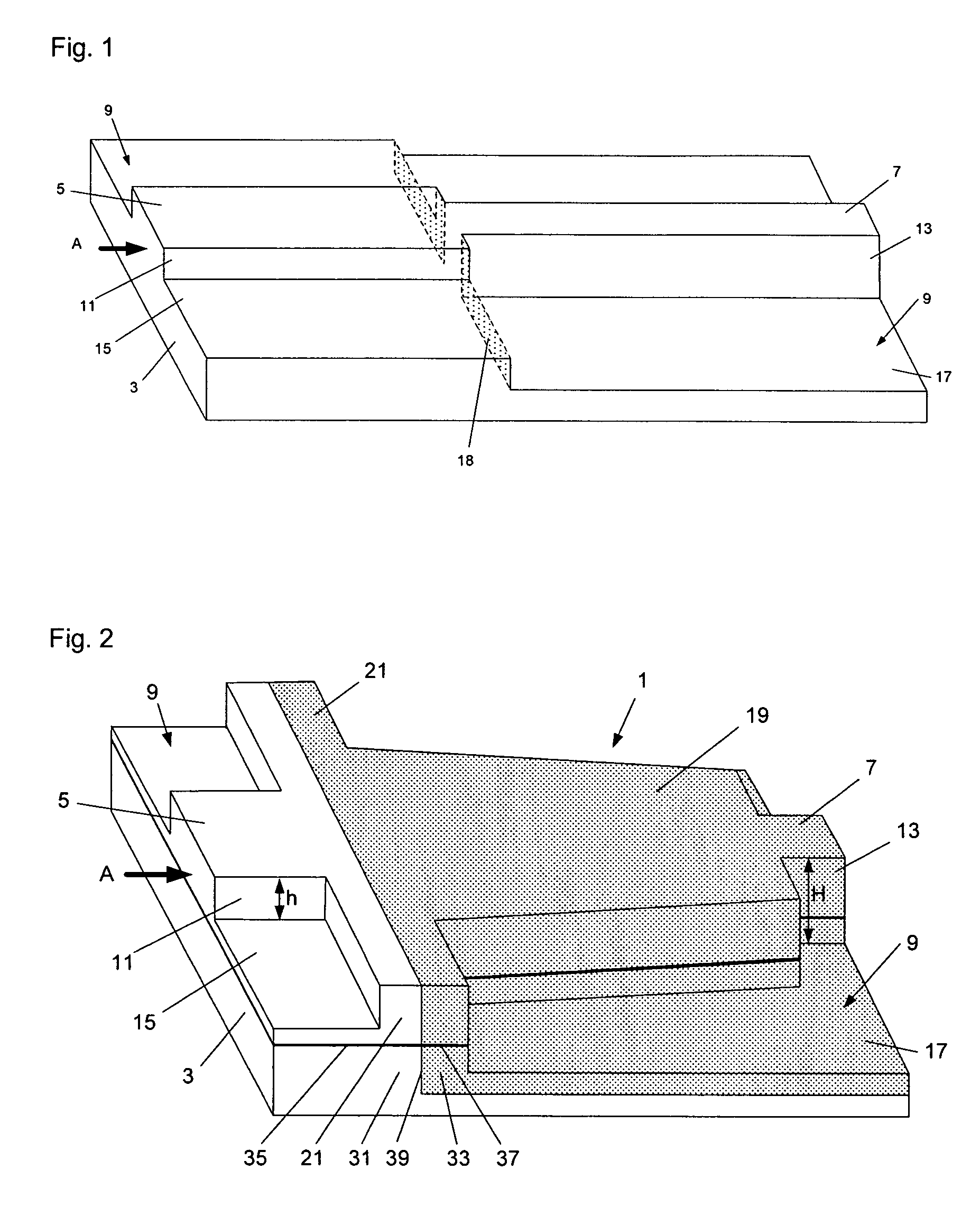
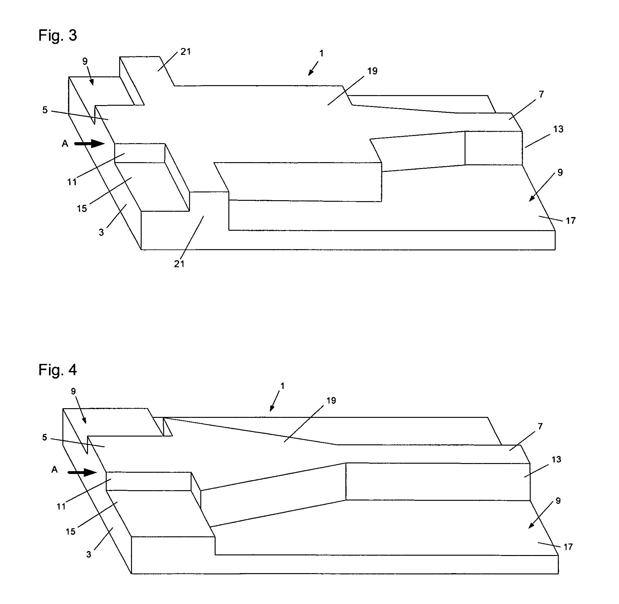
[0031]FIG. 1 shows, schematically, a known (prior art) type of optical device. FIG. 2 shows, schematically, an embodiment of an optical device 1 according to the present invention. Both the known type of optical device shown in FIG. 1, and the embodiment of the invention shown in FIG. 2 comprise a semiconductor structure 3 including a first ridge waveguide 5 and a second ridge waveguide 7. Each of the ridge waveguides comprises a ridge extending across a surface 9 of the semiconductor structure. The ridge 11 of the first ridge waveguide 5 has a first height h above a first region 15 of the surface 9 of the semiconductor structure. The ridge 13 of the second ridge waveguide 7 has a second, greater, height H above a second region 17 of the surface. The difference in heights between the ridges 11 and 13 is due to a difference in levels between the first and second regions 15 and 17 of the surface 9 of the semiconductor structure, i.e. the first region 15 is at a higher level than the s...


PUM


Abstract

An optical device comprises a semiconductor structure including first and second ridge waveguides, each waveguide comprising a ridge extending across a surface of the semiconductor structure. The ridge of the first waveguide has a first height above a first region of the surface, and the ridge of the second waveguide has a second, greater, height above a second region of the surface. The semiconductor structure includes a multimode interference (MMI) region situated between the first and second ridge waveguides, which provides a transition between them. At least a part of the MMI region is tapered in width and/or at least a part of the first and/or second ridge waveguide is tapered in width in a direction extending away from the MMI region.

Description

RELATED APPLICATION[0001]This application is a Continuation-in-part of U.S. patent application Ser. No. 11 / 267,400 filed Nov. 3, 2005, which is a Continuation-in-part of U.S. patent application Ser. No. 11 / 237,067 filed Sep. 27, 2005.FIELD OF THE INVENTION[0002]The present invention relates to semiconductor optical devices, and especially to integrated semiconductor optical devices in which a plurality of optically coupled components are fabricated in the same semiconductor structure (e.g. on the same semiconductor chip). The invention particularly concerns semiconductor optical devices including ridge (or rib) waveguides. (A ridge waveguide comprises a ridge extending across a surface of a semiconductor structure.)BACKGROUND ART[0003]A ridge waveguide typically comprises material remaining from an original uniform multi-layered planar waveguide whose layers are designed to confine light in-plane. The ridge is typically created by means of a selective etching process used to excavat...

Claims


Application Information

Patent Timeline
IPC IPC(8): H01S3/00
CPCG02B6/1228G02F1/025G02B6/2813G02F2001/217G02F1/217
Inventor WALKER, ROBERT GRAHAMPROSYK, KELVIN
Owner LUMENTUM TECH UK LTD
Why Eureka
Try Eureka