Semiconductor memory device

a memory device and semiconductor technology, applied in the field of semiconductor memory devices, can solve the problems of increased power consumption and activation of defective word lines, likely access time delay in relief operations, defective word lines may be activated, etc., to reduce access delays, improve reliability, and reduce access delays

Inactive Publication Date: 2007-02-27
HITACHI LTD +1
View PDF7 Cites 9 Cited by
  • Summary
  • Abstract
  • Description
  • Claims
  • Application Information

AI Technical Summary

Benefits of technology

[0011]In such a circumstance, an object of the present invention is to provide a semiconductor memory device capable of reducing the access delay due to the defect relief.
[0012]Also, another object of the present invention is to provide a semiconductor device capable of improving the reliability when driving a word line regardless of the defect relief and non-relief and capable of reducing the access delay due to the defect relief.
[0016]More specifically, since the sense amplifier of the redundant memory mat is not shared with the memory mat, the configuration of the redundant memory mat is separated from that of the normal memory mat. Also, since the shared circuit is omitted in the sense amplifier of the redundant memory mat, the capacitance of the second bit line can be reduced, and as a result, the data read speed in the redundant memory mat can be increased.
[0018]Therefore, the read signal amount to the second bit line of the redundant memory mat can be increased, and thus, the data read speed in the redundant memory mat can be increased. Note that the read speed can be further increased by using the omission of the shared circuit described above together with the reduction of the second bit line length.
[0019]Also, a semiconductor memory device according to the present invention comprises: a memory mat including a first word line, a first bit line, and a memory cell; a redundant memory mat including a second word line, a second bit line, and a memory cell and relieving defects in the memory mat by replacing the first word line with the second word line; a first sense amplifier region including a first sense amplifier for amplifying a signal of the first bit line and provided adjacent to the memory mat; a second sense amplifier region including a second sense amplifier for amplifying a signal of the second bit line and provided adjacent to the redundant memory mat; a circuit for determining relief or non-relief by comparing an address inputted externally with a predetermined relief address; a first start signal for starting the memory mat when the result of the determination circuit is the non-relief; and a second start signal for starting the redundant memory mat when the result of the determination circuit is the relief, wherein means for delaying generation timing of the second start signal from generation timing of the first start signal is provided, and means for increasing read speed of the redundant memory mat is provided so as to compensate the delay of the second start signal.
[0020]Therefore, the malfunction of the multiple selection caused by activating the normal memory mat and the redundant memory mat at the same time can be prevented, and the drive operation of the word line with high reliability can be realized. In addition, it is also possible to keep the same access time in the normal memory mat and the redundant memory mat.

Problems solved by technology

However, since both of the normal word line and the redundant word line are activated every time, there is the possibility that the problems of the increase in the power consumption and the activation of the defective word line are caused.
Also, in the operating method described in Japanese Patent Application Laid-Open No. 4-345998, not only the problem that the defective word line may be activated in the relief operation similar to that described above but also the problem of the access time delay in the relief operation probably occurs.

Method used


Image

  • Semiconductor memory device
  • Semiconductor memory device
  • Semiconductor memory device

Examples


Embodiment Construction

[0028]Hereinafter, embodiments of the present invention will be described in detail with reference to the accompanying drawings. Note that components having the same function are denoted by the same reference symbols throughout the drawings for describing the embodiment, and the repetitive description thereof will be omitted.

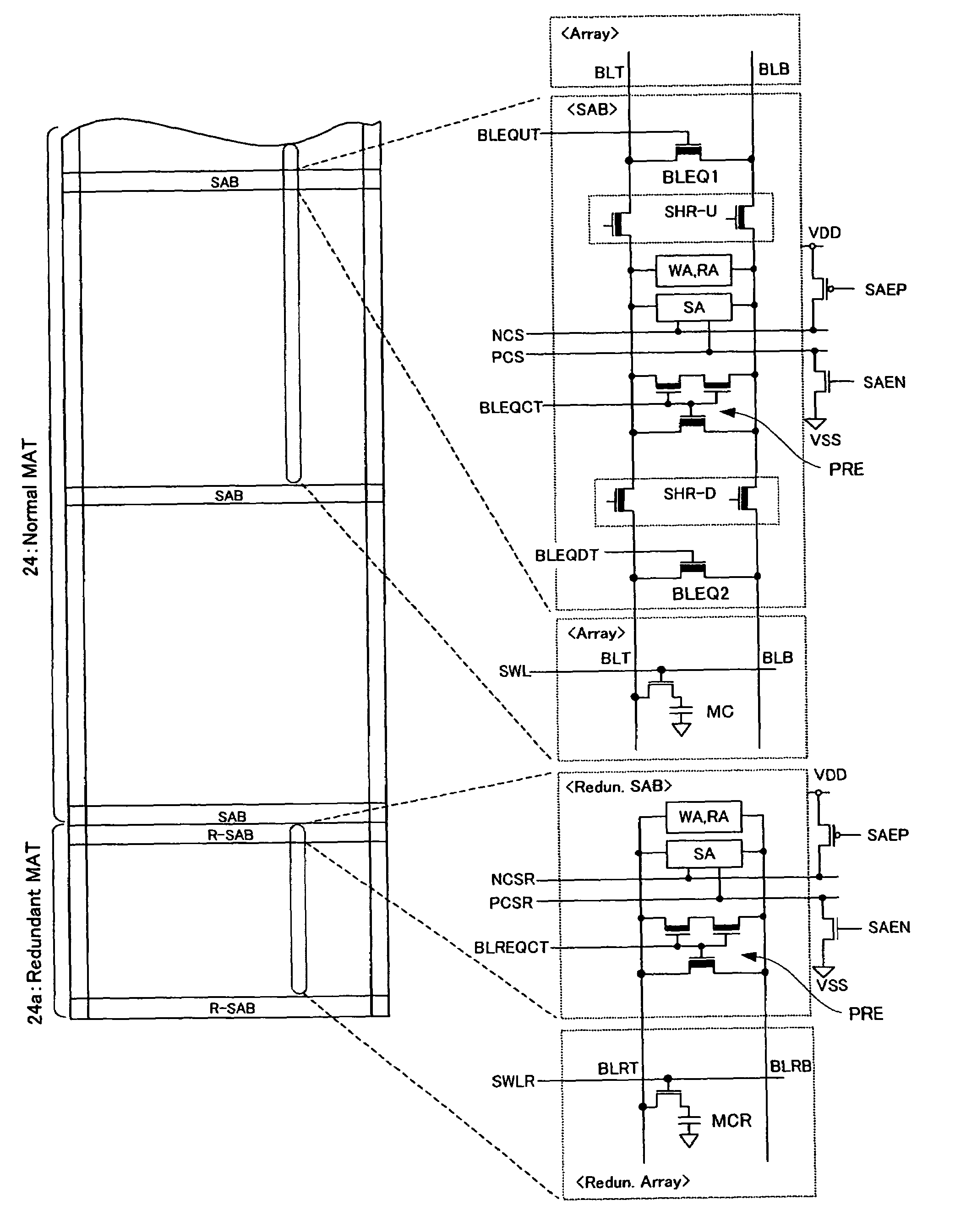
[0029]Also, in the description of the embodiment, a configuration example of a semiconductor memory device according to an embodiment of the present invention will be first described with reference to FIGS. 1 to 4, and then, an operation example of the semiconductor device will be described next with reference to FIGS. 5 and 6. In this case, the main characteristic of the present invention lies in the configuration of memory mat and the sense amplifier region described later with reference to FIGS. 3 and 4 and the operating method including the memory mat and the sense amplifier region described later with reference to FIGS. 5 and 6.

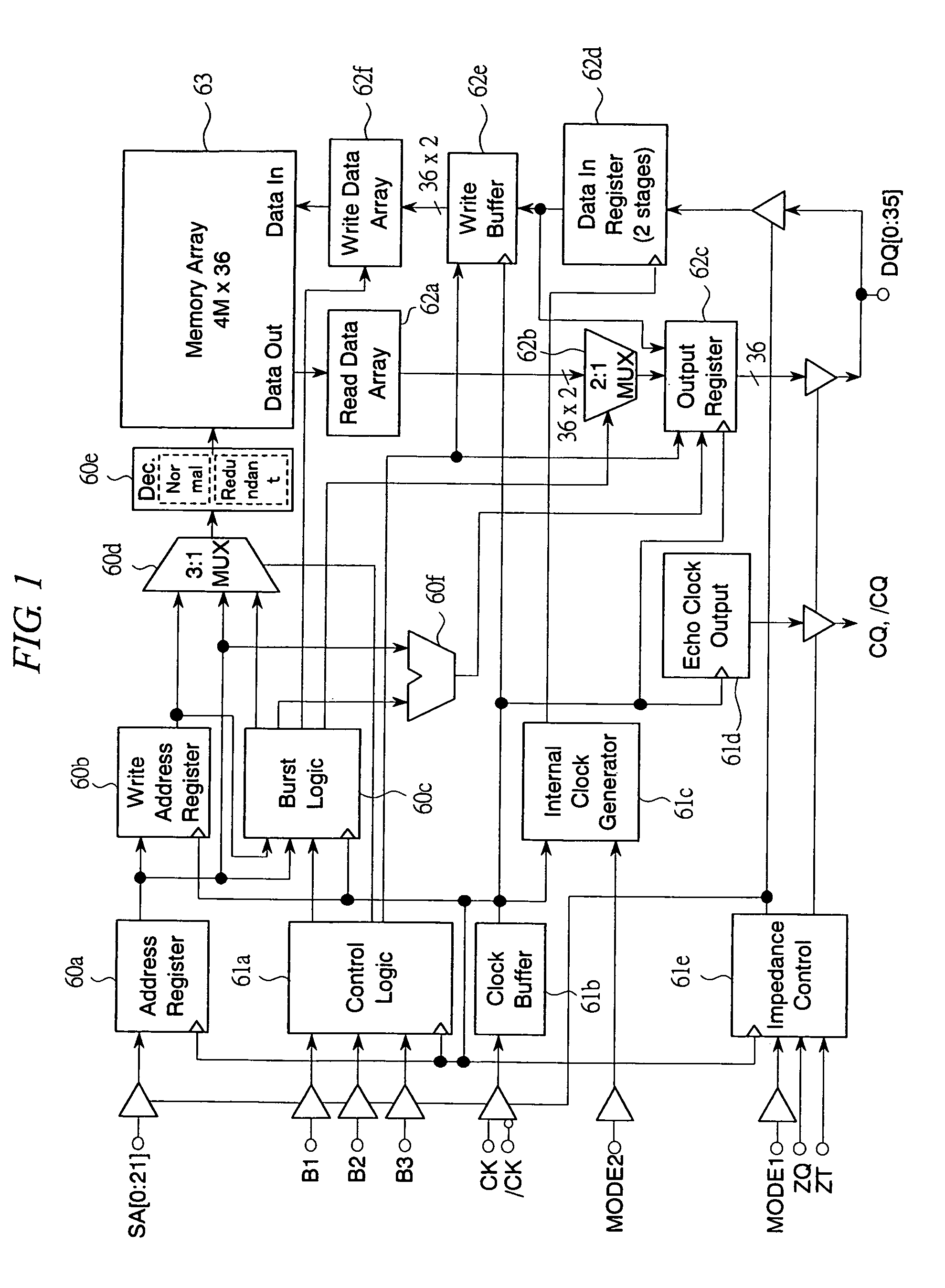
[0030]FIG. 1 is a block diagr...


PUM


Abstract

A semiconductor memory device capable of improving the reliability when driving a word line and capable of reducing the access delay due to the defect relief is provided. In order to prevent the multiple selection of a sub-word line of a normal memory mat and a sub-word line of a redundant memory mat, the start of the redundant memory mat is delayed from that of the normal memory mat, and in order to compensate the start delay, the shared circuit is eliminated and the bit line length is reduced in the redundant memory mat. By doing so, the read time of the bit lines is reduced and the signal amount is increased. Consequently, the same activation timing of the sense amplifier as that of the normal memory mat can be used also in the redundant memory mat.

Description

CROSS-REFERENCE TO RELATED APPLICATION[0001]The present application claims priority from Japanese Patent Application JP 2004-157191 filed on May 27, 2004, the content of which is hereby incorporated by reference into this application.TECHNICAL FIELD OF THE INVENTION[0002]The present invention relates to a semiconductor memory device. More particularly, the present invention relates to a technique effectively applied to a semiconductor memory device such as a dynamic RAM in which the high-speed operation is required also in a redundant memory array.BACKGROUND OF THE INVENTION[0003]According to the study by the inventors of the present invention, the technologies described below are known as the technologies for the defect relief in a memory.[0004]For example, the method of the operation for the defect relief of a word line described below is known. That is, the address is first confirmed and the decoding is performed after the confirmation, and then, the normal word line or the redun...

Claims


Application Information

Patent Timeline
Patent Type & Authority Patents(United States)
IPC IPC(8): G11C29/00G11C29/04G11C11/401G11C11/4091
CPCG11C29/84G11C11/4091G11C11/401
Inventor TAJIMA, KENICHIAKASAKI, HIROSHIHASEGAWA, MASATOSHITANAKA, YOUSUKE
Owner HITACHI LTD
Why Eureka
Try Eureka