Thermal interface material (TIM) with carbon nanotubes (CNT) and low thermal impedance
- Summary
- Abstract
- Description
- Claims
- Application Information
AI Technical Summary
Benefits of technology
Problems solved by technology
Method used
Image
Examples
Embodiment Construction
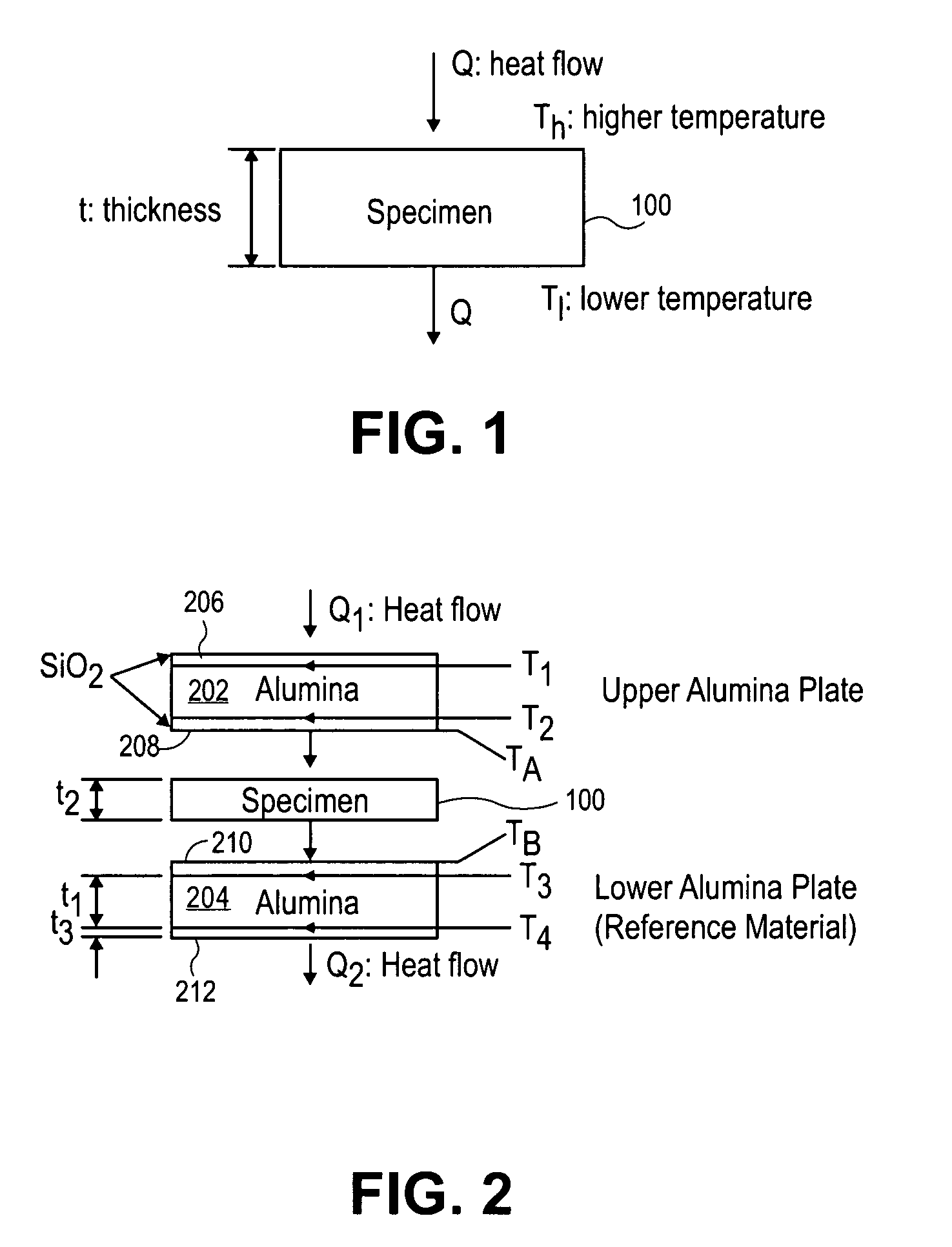
[0026]FIG. 1 is a schematic diagram illustrating a thermal interface material 100 (specimen) according to an embodiment of the present invention. The thermal interface material 100 includes a thickness (t), a high temperature (Th), a low temperature (Tl), and a heat flow (Q).
[0027]One-dimensional heat conduction under steady-state condition is given by:
[0028]QA=KΔTΔx(1)
where Q is the heat flow in watts, A, Δx and K are surface area, thickness and thermal conductivity of the thermal interface material 100, respectively, and ΔT is temperature difference between high temperature (Th) and low temperature (Tl).
[0029]Thermal resistance R (K / W) is defined from equation (1).
[0030]R=ΔTQ=Th-T1Q=tKA(2)
[0031]Sometimes, thermal impedance θ (Kcm2 / W) is a convenient property that is defined as:
[0032]θ=RA=tK(3)
[0033]FIG. 2 is a schematic diagram illustrating an apparatus 200 fabricated according to embodiments of the present invention. In the illustrated embodiment, the thermal interface mat...
PUM
| Property | Measurement | Unit |
|---|---|---|
| thickness | aaaaa | aaaaa |
| thickness | aaaaa | aaaaa |
| weight | aaaaa | aaaaa |
Abstract
Description
Claims
Application Information


