Memory function body, particle forming method therefor and, memory device, semiconductor device, and electronic equipment having the memory function body

a technology of memory function and particle forming method, which is applied in the direction of semiconductor devices, electrical devices, nanotechnology, etc., can solve the problems of increasing manufacturing time and labor, difficult to concurrently reduce the size of particles and the distance between particles to the nanometer order, and consuming a lot of time and labor. , to achieve the effect of reducing time and labor

Inactive Publication Date: 2007-03-06
SHARP KK
View PDF11 Cites 81 Cited by
  • Summary
  • Abstract
  • Description
  • Claims
  • Application Information

AI Technical Summary

Benefits of technology

[0010]Accordingly, an object of the present invention is to provide a memory function body capable of obtaining excellent characteristics and a p

Problems solved by technology

However, the method of forming the Si microcrystals on the silicon thermal oxide film through the annealing process has a problem that the manufacturing takes much time and labor since the process of depositing the silicon thermal oxide film is repeated.
Accordingly, there is a problem that in order to increase the area density of the Si particles, a number of repetitions of the process steps from the step of depositing the silicon thermal oxide film to the

Method used


Image

  • Memory function body, particle forming method therefor and, memory device, semiconductor device, and electronic equipment having the memory function body
  • Memory function body, particle forming method therefor and, memory device, semiconductor device, and electronic equipment having the memory function body
  • Memory function body, particle forming method therefor and, memory device, semiconductor device, and electronic equipment having the memory function body

Examples


first embodiment

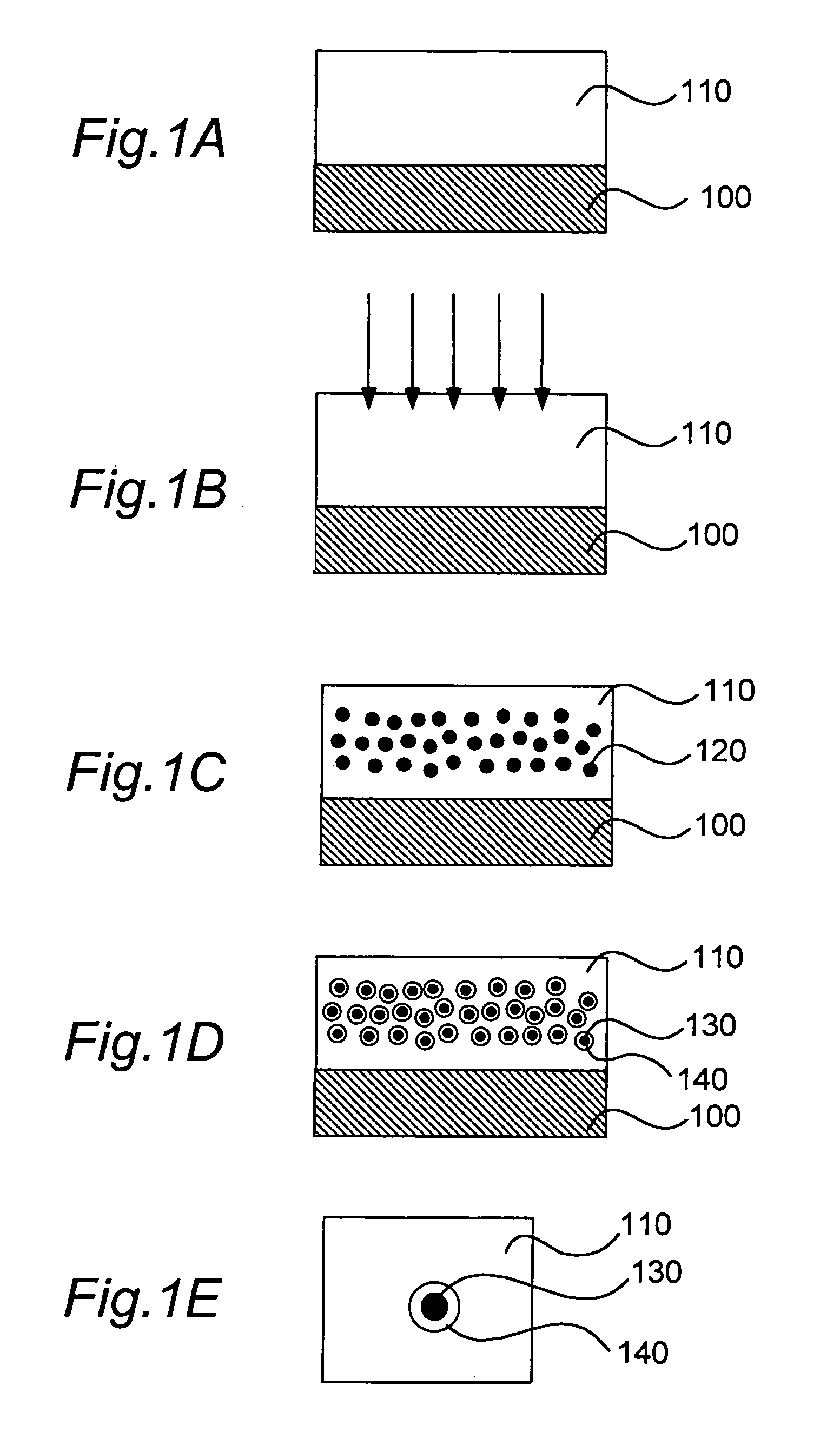
[0073](First Embodiment)

[0074]FIGS. 1A through 1E are process charts showing a particle manufacturing method according to a first embodiment of the present invention. In the present embodiment, silver particles as conductive particles are formed in a silicon oxide film that serves as an insulator.

[0075]First, as shown in FIG. 1A, a silicon oxide film 110 that serves as an insulator is formed on a top surface of a silicon substrate 100 that serves as a semiconductor substrate through a thermal oxidation process. In the present embodiment, the film is formed to a film thickness of about 50 nm.

[0076]Next, as shown in FIG. 1B, silver as a substance for forming conductive particles is introduced into the silicon oxide film 110 by the ion implantation method. At this time, the distribution of implantation tends to expand excessively if implantation energy is extremely high. Thus, such a high implantation energy is not suitable for the implantation into the comparatively thin silicon oxide...

second embodiment

[0091](Second Embodiment)

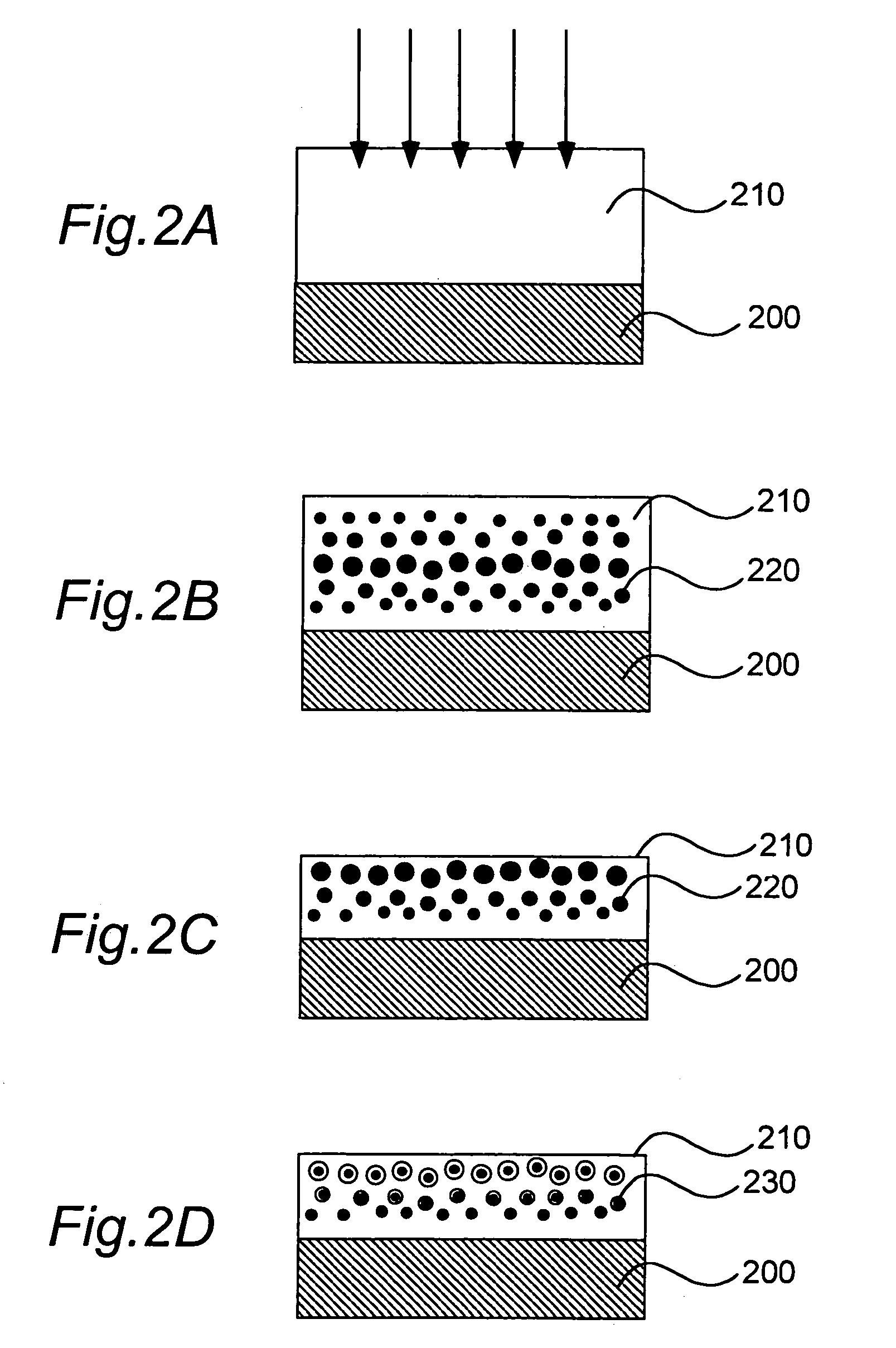
[0092]In a particle forming method of a second embodiment, an etching process is further provided between the particle forming process and the insulation process as carried out in the particle forming method of the first embodiment, so that a region from the top surface of the insulator in which the particles have been formed to the prescribed depth is removed.

[0093]In the present embodiment, silver particles are formed as conductive particles similarly to the first embodiment.

[0094]First, as shown in FIG. 2A, a silicon oxide film 210 that serves as an insulator is formed on a top surface of a silicon substrate 200 that serves as a semiconductor substrate through a thermal oxidation process. In the present embodiment, the film is formed to a film thickness of about 100 nm.

[0095]Next, as shown in FIG. 2B, silver is introduced into the silicon oxide film 210 by the ion implantation method. In this case, the implantation energy is set so that the implantation d...

third embodiment

[0100](Third Embodiment)

[0101]In a third embodiment, an etching process is provided between an ion implantation process and a heat treatment process, and a region from a surface to a prescribed depth is removed from an insulator in which a substance for forming conductive particles has been implanted.

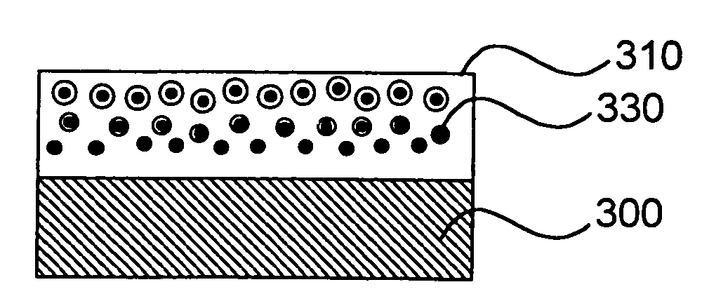
[0102]In the present embodiment, silver particles that serve as conductive particles are formed in a silicon oxide film that serves as an insulator.

[0103]First, a silicon oxide film 310 as an insulator is formed on a surface of a silicon substrate 300 as a semiconductor substrate through a thermal oxidation process. In the present embodiment, the film is formed to a film thickness of about 100 nm.

[0104]Next, as shown in FIG. 3A, silver is introduced into the silicon oxide film 310 by the ion implantation method. In this case, the implantation energy is set so that the implantation depth becomes about 50 nm.

[0105]In this case, the implantation concentration of silver ions forms a concent...


PUM


Abstract

A memory function body has a medium interposed between a first conductor (e.g., a conductive substrate) and a second conductor (e.g., an electrode) and consisting of a first material (e.g., silicon oxide or silicon nitride). The medium contains particles. Each particle is covered with a second material (e.g., silver oxide) and formed of a third material (e.g., silver). The second material functions as a barrier against passage of electric charges, and the third material has a function of retaining electric charges. The third material is introduced into the medium by, for example, a negative ion implantation method.

Description

[0001]This nonprovisional application claims priority under 35 U.S.C. §119(a) on Patent Application No. 2003-067659 filed in Japan on Mar. 13, 2003, the entire contents of which are hereby incorporated by reference.BACKGROUND OF THE INVENTION[0002]The present invention relates to a memory function body, a method for forming, for example, nanometer-size particles for use in this memory function body, a memory device, a semiconductor device and electronic equipment.[0003]In recent years, as ultramicro electronic equipment that employs a nanometer-size particle or particles, there have been proposed, for example, a single-electron transistor and a memory that contains a particle or particles called the “nanodot” or “nanocrystal” in a gate insulation film.[0004]As a method for forming such a particle for the electronic equipment, there is proposed a method that, to form a Si (silicon) particle, deposits amorphous silicon on a silicon thermal oxide film by the LPCVD (Low Pressure Chemica...

Claims


Application Information

Patent Timeline
IPC IPC(8): H01L21/8238H01L21/265H01L21/28H01L21/8247H01L27/115H01L29/423H01L29/788H01L29/792
CPCB82Y10/00H01L29/42332H01L21/28273H01L29/40114
Inventor ARAI, NOBUTOSHIIWATA, HIROSHIKAKIMOTO, SEIZO
Owner SHARP KK
Why Eureka
Try Eureka