Electrostatic discharge conduction device and mixed power integrated circuits using same

a technology of esd conduction device and mixed power integrated circuit, which is applied in the direction of electromagneticonductor device, emergency protective arrangement for limiting excess voltage/current, electrical apparatus, etc., can solve the problem that the esd conduction path of mixed power integrated circuits may not be sufficient in some configurations, weakening, and damage to devices, etc. problem, to achieve the effect of low leakage curren

Active Publication Date: 2007-03-06
MACRONIX INT CO LTD
View PDF13 Cites 30 Cited by
  • Summary
  • Abstract
  • Description
  • Claims
  • Application Information

AI Technical Summary

Benefits of technology

[0015]The conduction device in a basic configuration taught by the present invention comprises a diode in series with a NMOS transistor, having a p-type ring (“p-ring”) surrounding the source and drain of the NMOS transistor, coupled as a conduction device between supply conductors. An SCR path in the substrate is enabled by a control circuit in response to an ESD event. During normal operation, the device does not conduct noise between the supply conductors, and allows only very low leakage current. During an ESD event, the SCR is triggered. The SCR establishes a low voltage drop path having a low holding voltage when conducting, providing for efficient discharge of the ESD event. In multi-power integrated circuits, the conduction device can be used to connect the power supply buses in the multiple power domains by highly conductive paths during an ESD event.

Problems solved by technology

Although this arrangement works suitably in some environments, a weakness is induced because of the finite resistance of the ESD conduction cells, symbolized by the resistor symbol within the block of ESD cell 20.
However if the resistance in the ESD conduction cell 20 is too high, and the voltage difference caused is high enough to overstress and damage devices in the internal circuit 11, then the ESD current may discharge along Path 2, further damaging the device.
Thus, as can be seen, mixed power integrated circuits may lack sufficient ESD discharge paths in some configurations.

Method used


Image

  • Electrostatic discharge conduction device and mixed power integrated circuits using same
  • Electrostatic discharge conduction device and mixed power integrated circuits using same
  • Electrostatic discharge conduction device and mixed power integrated circuits using same

Examples


Embodiment Construction

[0026]A detailed description of embodiments of the present invention is provided with reference to the FIGS. 4–9.

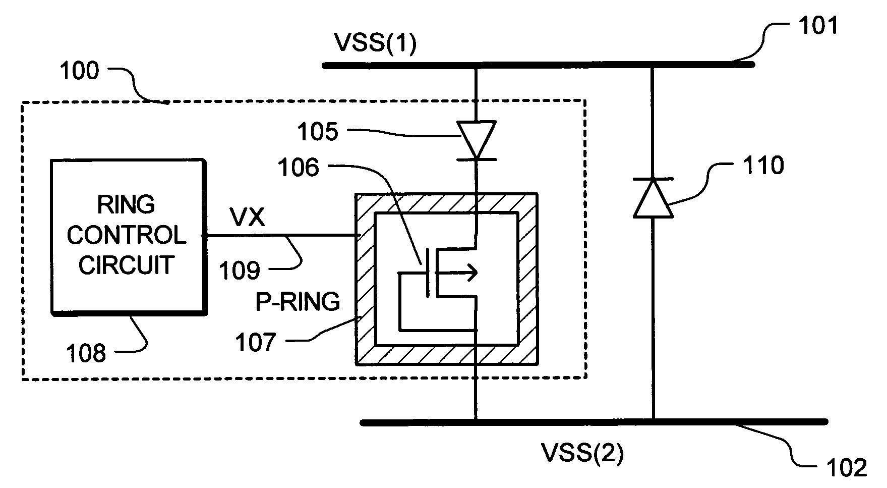
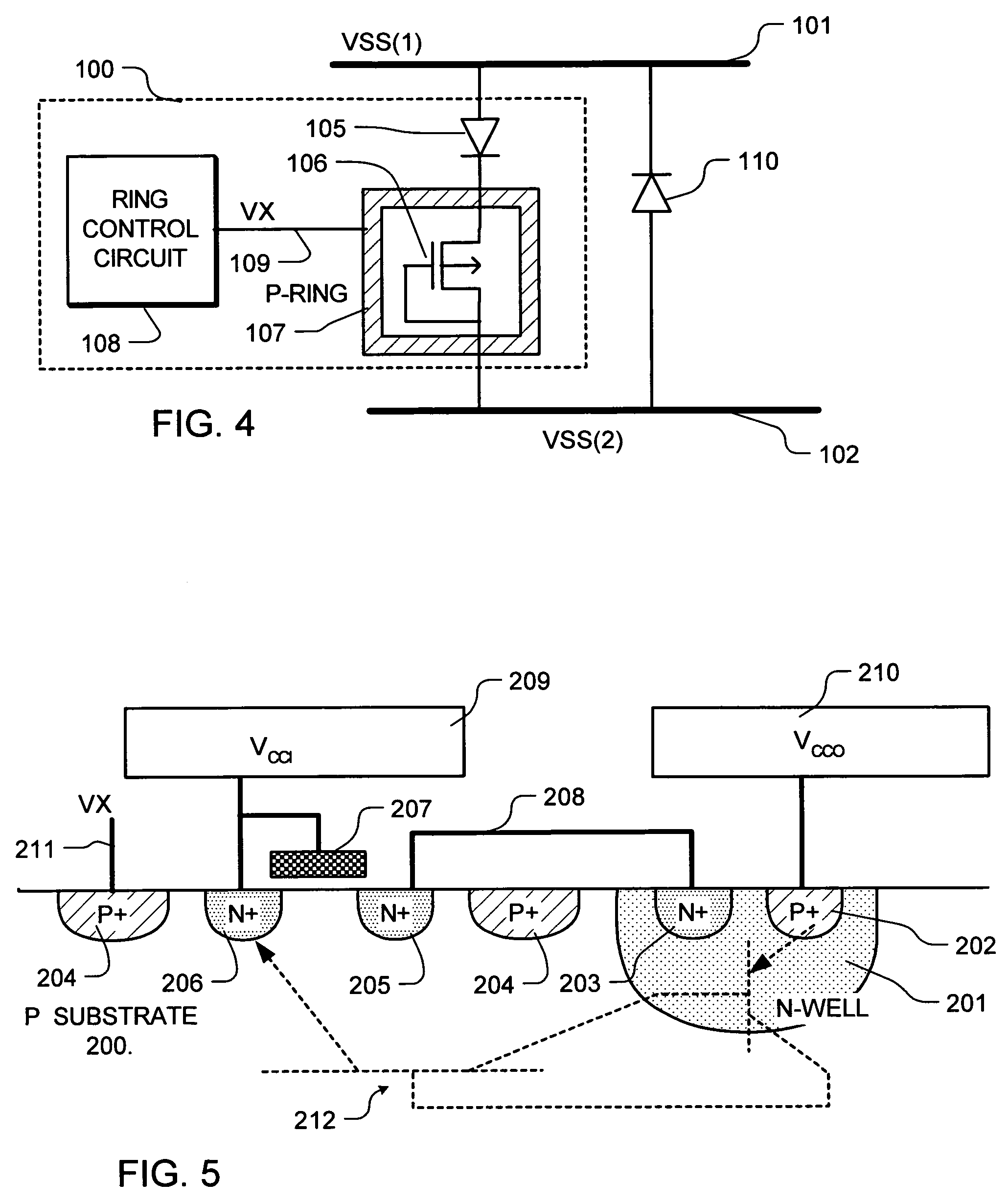
[0027]FIG. 4 shows a conduction device 100 connected between a first conductor 101 and a second conductor 102, where the first conductor 101 and second conductor 102 are arranged to carry voltages that are close to one another. For example, the first conductor 101 and second conductor 102 comprise voltage supply buses for ground potentials VSS(1) and VSS(2) in the illustrated embodiment. In other examples, the first conductor 101 and second conductor 102 are voltage supply buses for the supply potentials VCC(1) and VCC(2) for separate power domains in an integrated circuit.

[0028]The conduction device includes a diode 105 and a transistor 106. The anode of the diode 105 is connected to the first conductor 101, and the cathode of the diode 105 is connected to the drain of the transistor 106. The gate and the source of the transistor 106 are connected to the second conductor...


PUM


Abstract

A device for connection between supply buses in mixed power integrated circuits includes a diode in series with a transistor with an active p-ring in a semiconductor substrate. The active p-ring surrounds the source and drain of the transistor with a conductive region having the same conductivity type as the semiconductor substrate. A control circuit coupled to the p-ring applies a bias voltage in response to an ESD event affecting the first and second conductors. The bias voltage tends to inject carriers into the semiconductor substrate which enables discharge of the short voltage pulse via a parasitic SCR in the substrate from the anode of the diode to the source of the transistor.

Description

BACKGROUND OF THE INVENTION[0001]1. Field of the Invention[0002]The present invention relates to electrostatic discharge ESD conduction devices for mixed power integrated circuits, particularly for providing noise isolation and ESD conduction between power buses having similar voltage levels in such mixed power integrated circuits.[0003]2. Description of Related Art[0004]Mixed power integrated circuits are being developed for a wide variety of applications. Such integrated circuits include circuits that operate based on different power supply arrangements. Mixed power integrated circuits can be characterized as including multiple power domains, where a power domain comprises circuits coupled to a power supply bus network that is separated from the power supply bus networks of other domains. For example, integrated circuits having digital circuits and analog circuits often provide a digital domain having a digital power supply bus network with both digital power and digital ground bu...

Claims


Application Information

Patent Timeline
Patent Type & Authority Patents(United States)
IPC IPC(8): H02H9/00
CPCH01L27/0292H01L27/0251
Inventor SU, SHINLAI, CHUN-HSIANGLU, CHA-LINGYEH, YEN-HUNGLU, TAO-CHENG
Owner MACRONIX INT CO LTD
Why Eureka
Try Eureka