Reduced size transmission line using capacitive loading

a transmission line and capacitive loading technology, applied in the direction of impedence networks, waveguide devices, electrical equipment, etc., can solve the problems of difficult modeling, high frequency impedance, and inability to meet the requirements of the transmission line, so as to achieve size-reduced physical compactness and increase the electrical length of the uniplanar transmission line

Inactive Publication Date: 2007-03-13
HER MAJESTY THE QUEEN & RIGHT OF CANADA REPRESENTED BY THE MIN OF IND THROUGH THE COMM RES CENT
View PDF3 Cites 11 Cited by
  • Summary
  • Abstract
  • Description
  • Claims
  • Application Information

AI Technical Summary

Benefits of technology

[0016]It is another object of this invention to provide a method of increasing electrical length of a uniplanar transmission line by capacitively loading thereof using TFMS stubs for use in size-reduced physically compact microwave circuits.

Problems solved by technology

MIM capacitors at high frequencies, for example, in microwave and millimeter-wave wavelength regions, can be difficult to model and may be susceptible to fabrication process deviations.
In these instances, the electrical performance of a size-reduced transmission line may be negatively affected.
Standard microstrip stubs suffer from at least two negative aspects that limit a total amount of size reduction.
Secondly, standard microstrip stubs must be placed far enough apart to prevent electromagnetic coupling between them, usually at least a substrate thickness apart.
This minimum spacing also limits the total amount of size-reduction.
Nonetheless, size-reduction using uniplanar stubs is still limited by their minimum realizable characteristic impedance and a minimum spacing between them required for electromagnetic isolation.

Method used


Image

  • Reduced size transmission line using capacitive loading
  • Reduced size transmission line using capacitive loading
  • Reduced size transmission line using capacitive loading

Examples


Embodiment Construction

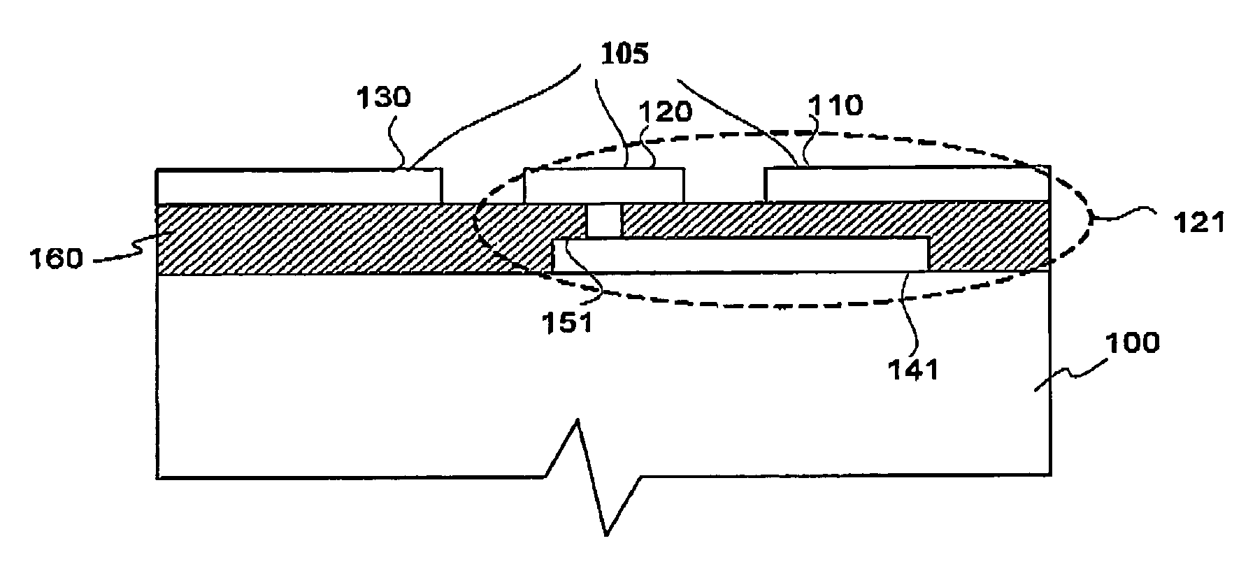
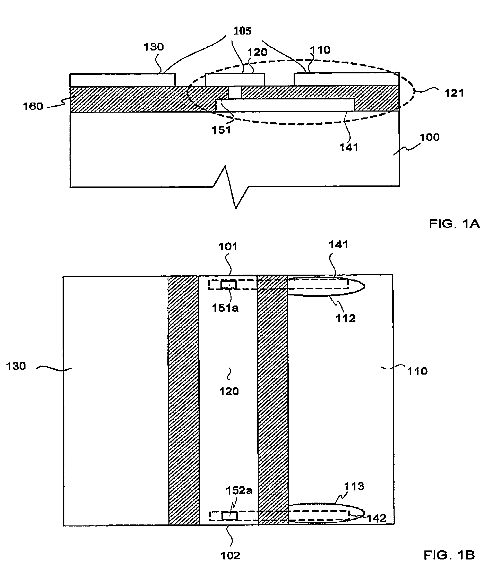
[0050]A first exemplary embodiment of a passive network of the present invention is a multi-layer capacitively loaded transmission line which is shown in FIGS. 1A and 1B, which will now be discussed.

[0051]With reference to FIG. 1A, a first uniplanar transmission line (UTL) 105 is embodied as a coplanar waveguide (CPW) formed by a signal conductor 120 and two ground conductors 130 and 110 on a thin dielectric film 160 supported by a substrate 100. The thin dielectric film 160 can be a single layer of a dielectric material or be formed by multiple layers of dielectric materials. The signal conductor 120 is disposed between the ground conductors 130 and 110 at a distance therefrom, and is typically narrower than the ground conductors. The top view of the first UTL 105 is shown in FIG. 1B, also showing a first end 101 and a second end 102 thereof for connecting to other elements of a larger microwave circuit such as input / output ports, other transmission lines, antennas, transistors etc...


PUM


Abstract

A capacitively loaded multilevel transmission line network for operation at a microwave frequency f is disclosed wherein microstrip conductors are disposed over or under a uniplanar transmission line (UTL), electrically connected thereto at or near opposing ends of the UTL and coupled to portions of the UTL separated therefrom by a thin dielectric film. The microstrip conductors and the portions of the UTL coupled thereto form thin-film microstrip (TFMS) shunt stubs capacitively loading the ends of the UTL for increasing its electrical length. The present invention enables considerable size reduction of microwave circuits having uniplanar transmission lines.

Description

CROSS-REFERENCE TO RELATED APPLICATIONS[0001]N / AFIELD OF THE INVENTION[0002]The present invention relates generally to transmission line structures in microwave circuits and more particularly to multilayer transmission line structures that are capacitively loaded for the purpose of circuit size reduction.BACKGROUND OF THE INVENTION[0003]Transmission line structures in microwave circuits are often a large part of the overall circuit size. Since the cost of a microwave circuit generally increases as its size increases, minimizing the size of transmission line structures can be of significant importance for many applications of microwave circuits.[0004]Physical size of a transmission line is usually governed by its desired electrical characteristics, and in many cases—by a target electrical length of the transmission line. The electrical length of a transmission line is proportional to a ration of its physical length to a wavelength of the guided electromagnetic mode propagating along ...

Claims


Application Information

Patent Timeline
Patent Type & Authority Patents(United States)
IPC IPC(8): H01P5/02
CPCH01P3/081
Inventor HETTAK, KHELIFA
Owner HER MAJESTY THE QUEEN & RIGHT OF CANADA REPRESENTED BY THE MIN OF IND THROUGH THE COMM RES CENT
Why Eureka
Try Eureka