Laser-to-fiber coupling

a fiber coupling and fiber technology, applied in the field of devices and/or methods of making electrically pumped chiplaserdiodes, can solve the problems of low output power, low volume of vcsel, and reduced performance of vcsel, so as to reduce or even eliminate the need for expensive discrete optical elements, reduce alignment problems, and avoid noise reflections carefully controlled

Inactive Publication Date: 2007-03-20
RES FOUND OF THE CENT FLORIDA UNIV OF THE +1
View PDF35 Cites 37 Cited by
  • Summary
  • Abstract
  • Description
  • Claims
  • Application Information

AI Technical Summary

Benefits of technology

[0008]Our wafer scale processing techniques produce chip-laser-diodes with a diffraction grating that redirects output light out the top and/or bottom surfaces. Noise reflections are preferably carefully controlled, allowing significant reduction of the signal fed to the active region. Combination gratings and additional gratings and/or integrated lenses on the top or bottom of the diode can also be made utilizing wafer scale processes, reducing or even elimina

Problems solved by technology

VCSELs, however, have had substantially reduced performance and a complicated device structure that does not effectively translate across the dif

Method used


Image

  • Laser-to-fiber coupling
  • Laser-to-fiber coupling
  • Laser-to-fiber coupling

Examples


Embodiment Construction

[0037]The making and using of the presently preferred embodiments are discussed in detail below. It should be appreciated, however, that the present invention provides many applicable inventive concepts that can be embodied in a wide variety of specific contexts. The specific embodiments discussed are merely illustrative of specific ways to make and use the invention, and do not limit the scope of the invention.

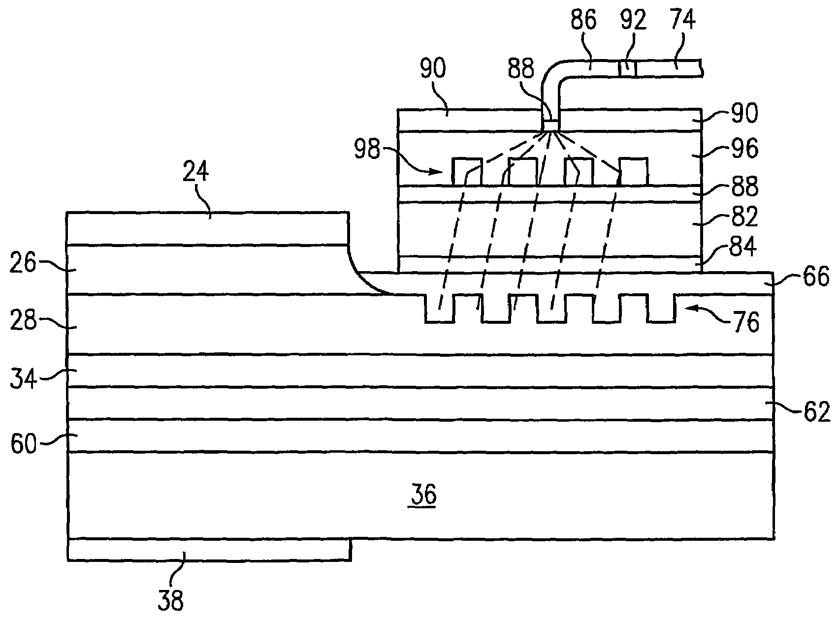
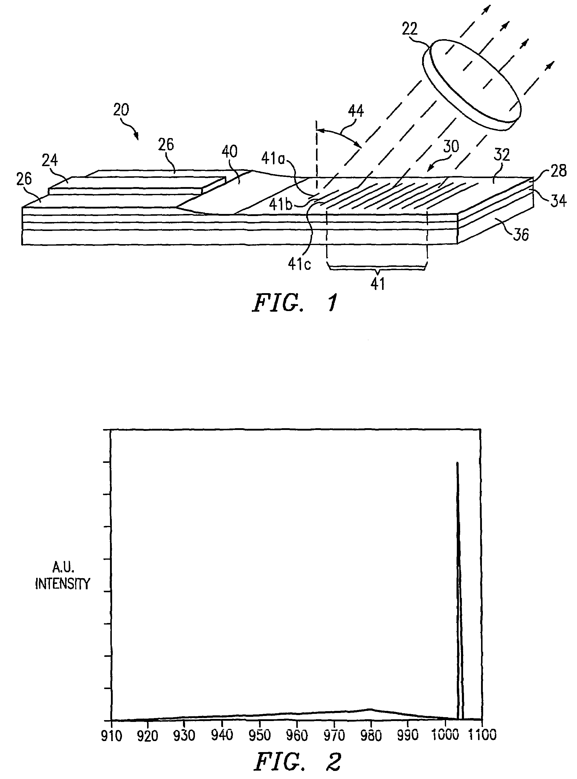
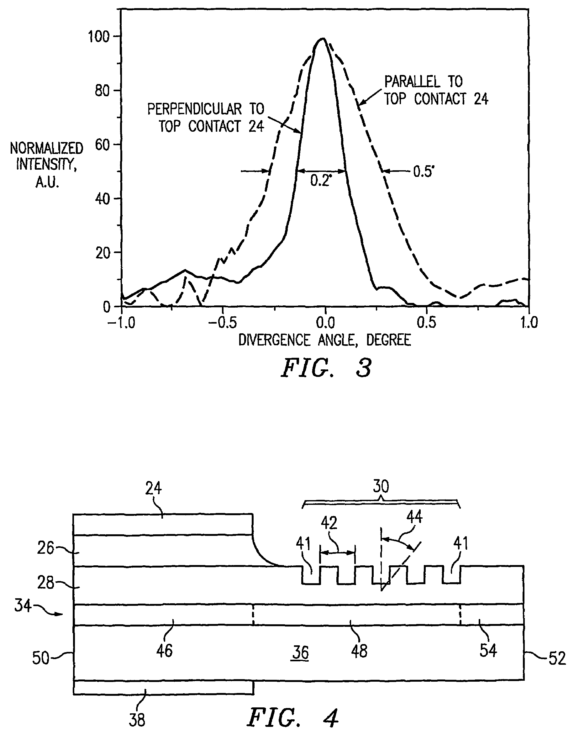
[0038]This diode-chip-laser can provide narrow-band coherent light, (light that is virtually all in-phase and at, or essentially at, the same wavelength). These grating-coupled diode improvement enable, for the first time, combining of all the functional advantages of non-semiconductor-chip (e.g., fluid) lasers with the efficiency, economy, convenience, and the efficiencies of semiconductor-chip-manufacturing (wafer processing). These chips generate light parallel to the top surface and utilize gratings that diffract light out top and / or bottom surfaces. Thus they have both a...


PUM


Abstract

Our wafer scale processing techniques produce chip-laser-diodes with a diffraction grating (78) that redirects output light out the top (88) and/or bottom surfaces. Generally, a diffraction grating (78) and integrated lens-grating (78) are used herein to couple light from the chip to an output fiber (74), and the lens-grating (78) is spaced from the diffraction grating (76). Preferably the diffraction grating (76) and integrated lens grating (78) are also used to couple light from the output fiber (74) back to the active region of the chip. The integrated lens-grating (78) can be in a coupling block (82). The use of a coupling block (82) can eliminate “facet-type damage”. A coupling block (82) is generally used herein to couple light from the chip to an output fiber (74), and preferably to couple feedback reflected from the fiber (74) back to the chip.

Description

[0001]This application claims the priority benefit of the following U.S. Provisional Applications: Ser. No. 60 / 277,885, entitled ADVANCED LASER DIODE, filed on Mar. 22, 2001; Ser. No. 60 / 293,903, entitled LONG CAVITY LASER DIODE, filed on May 25, 2001; Ser. No. 60 / 293,905, entitled SLANTED FINGER LASER DIODE GRATING, filed on May 25, 2001; Ser. No. 60 / 293,907, entitled NON-REFLECTIVE TOP LASER DIODE CONTACT, filed on May 25, 2001; Ser. No. 60 / 293,904, entitled ETCH STOP FOR LASER DIODE, filed on May 25, 2001; Ser. No. 60 / 293,906, entitled ION IMPLANTED LASER DIODE GRATING, filed on May 25, 2001; Ser. No. 60 / 293,814, entitled PARTIALLY-DOPED LASER DIODE GRIN, filed on May 25, 2001; Ser. No. 60 / 293,740, entitled TUNGSTEN CONTACT FOR LASER DIODE, filed on May 25, 2001; Ser. No. 60 / 315,160, entitled ADVANCED GRATING-COUPLED LASER DIODE, filed on Aug. 27, 2001; Ser. No. 60 / 344,941, entitled ADVANCED GRATING-COUPLED LASER DIODE, filed on Dec. 21, 2001; Ser. No. 60 / 344,972, entitled COUPLE...

Claims


Application Information

Patent Timeline
IPC IPC(8): H01S3/08H01S5/026G02B6/34G02B6/42H01S5/00H01S5/042H01S5/12H01S5/14H01S5/187
CPCG02B6/34G02B6/4214H01S5/026H01S5/141H01S5/187H01S5/02284H01S5/0267H01S5/0425H01S2301/185H01S5/1014H01S5/1231H01S5/2027H01S5/0655H01S2301/176H01S5/04254H01S5/02251
Inventor BULLINGTON, JEFF A.STOLTZ, RICHARD A.VAISSIE, LAURENTJOHNSON, ERIC G.MOHARAM, M. GAMAL
Owner RES FOUND OF THE CENT FLORIDA UNIV OF THE
Why Eureka
Try Eureka