Etching process and patterning process

a patterning and etching technology, applied in the field of etching process, can solve the problems of increasing the degree of pattern distortion, difficult control of critical dimensions, and easy distorted photoresist patterns, and achieve the effect of accurate pattern transfer

Active Publication Date: 2007-03-27
UNITED MICROELECTRONICS CORP
View PDF8 Cites 5 Cited by
  • Summary
  • Abstract
  • Description
  • Claims
  • Application Information

AI Technical Summary

Benefits of technology

[0007]In view of the foregoing, this invention provides an etching process that includes a polymer removal step to keep the critical dimension unchanged and make the pattern transfer accurate.
[0013]Furthermore, the patterned photoresist layer can be trimmed to reduce its linewidth after the material layer having the patterned photoresist layer thereon is provided.
[0014]Since the polymer generated in the etching step of the BARC is removed in the subsequent cleaning step, the photoresist patterns can be accurately transferred to the material layer in the latter etching step of the material layer.
[0019]Since the linewidth of photoresist patterns is reduced with the trimmed step and the polymer generated in the subsequent etching step of the BARC is removed, the linewidth of the patterns transferred to the material layer can be reduced.

Problems solved by technology

However, since light having a shorter wavelength has higher reflectivity at the interface of the photoresist layer and the die, the resulting photoresist patterns are distorted more easily.
The problem is even more significant when a layer of high-reflectivity material, such as, polysilicon or metal like aluminum, is to be patterned, since the degree of pattern distortion increases with the intensity of the reflective light.
Accordingly, when the process linewidth is small and the reflectivity of the film to be patterned is high, controlling the critical dimension is particularly difficult.
Therefore, in the latter step of etching the material layer, the patterns transferred to the material layer and the critical dimension thereof are not correct.

Method used


Image

  • Etching process and patterning process
  • Etching process and patterning process
  • Etching process and patterning process

Examples


Embodiment Construction

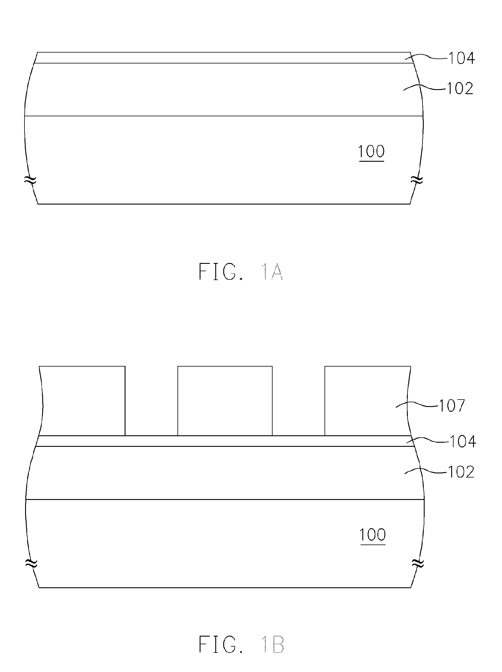
[0022]Referring to FIG. 1A, a substrate 100 having a material layer 102 to be etched thereon is provided, and a BARC 104 is formed on a material layer 102.

[0023]The material layer 102 may be a polysilicon layer.

[0024]The BARC 104 may include an inorganic material or an organic material. The inorganic material can be formed with chemical vapor deposition (CVD), and may be amorphous carbon, silicon nitride, silicon oxynitride or titanium oxide.

[0025]Referring to FIG. 1B, a patterned photoresist layer 107 is formed on the BARC 104. The method for forming the patterned photoresist layer 107 may include the following steps. A photoresist layer is formed on the BARC 104 with spin-coating and baking, and is then patterned using a lithography method. The material solution for coating the photoresist layer includes a resin, a solvent and a photosensitive agent.

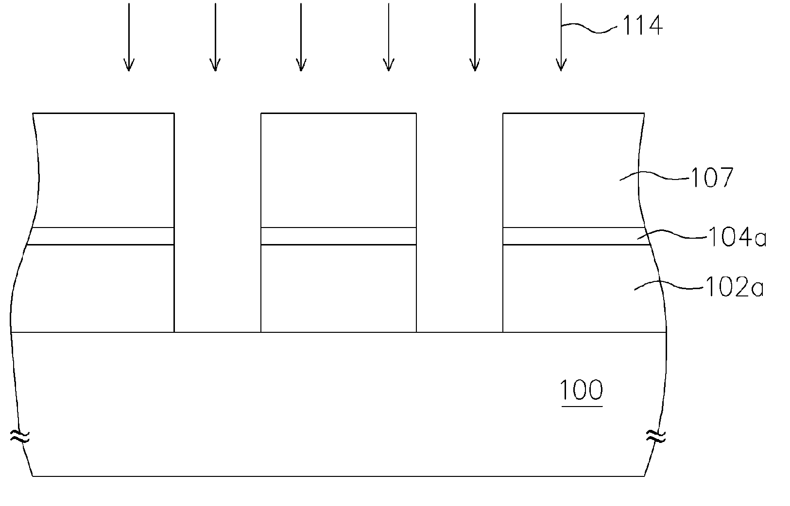
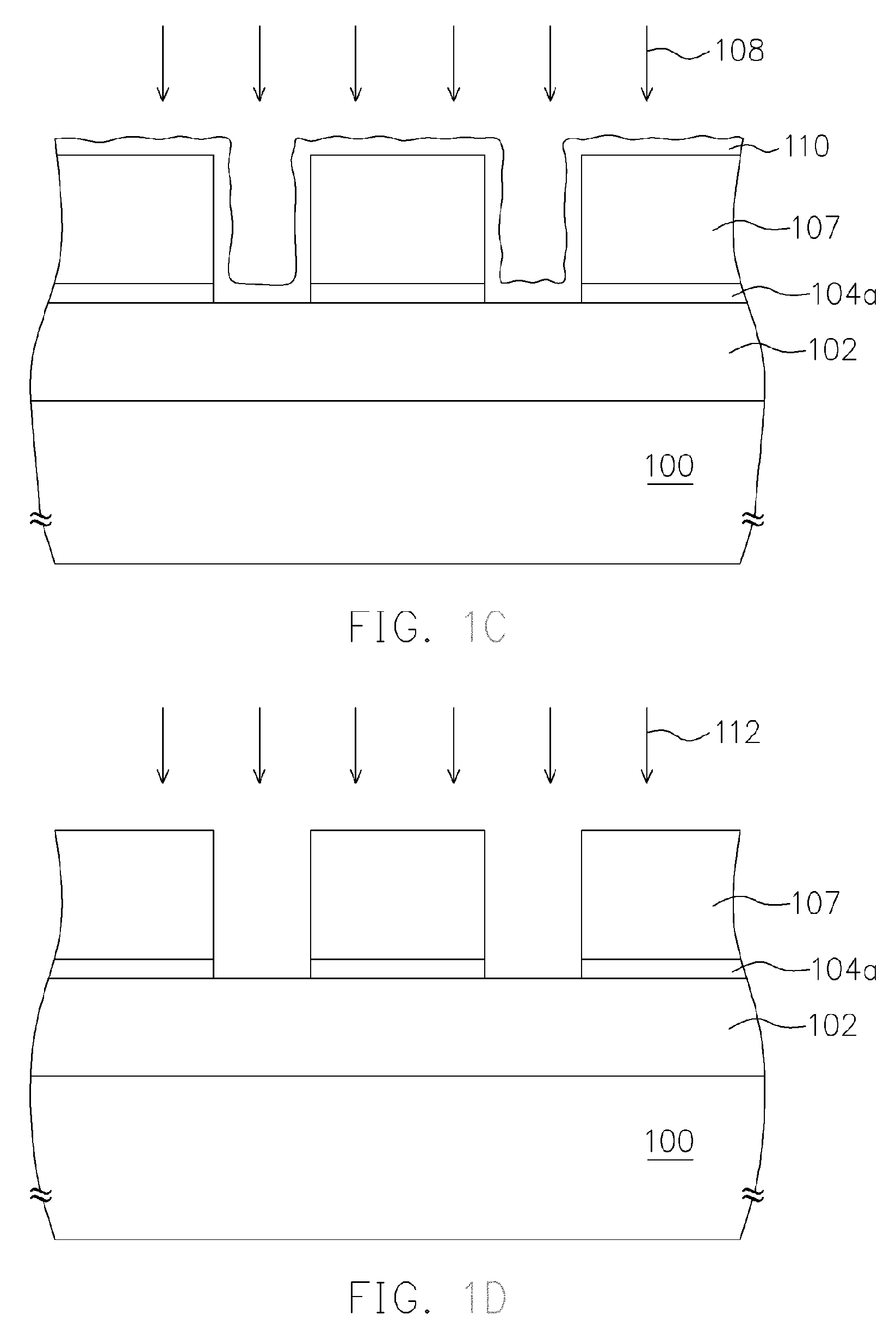
[0026]Referring to FIG. 1C, an etching step 108 is performed to the BARC 104 using the patterned photoresist layer 107 as a mask, so ...


PUM

PropertyMeasurementUnit
organicaaaaaaaaaa
wavelengthaaaaaaaaaa
reflectivityaaaaaaaaaa

Abstract

An etching process is described. A material layer having a bottom anti-reflection coating (BARC) and a patterned photoresist layer thereon is provided. An etching step is performed to the BARC using the patterned photoresist layer as a mask. A cleaning step is performed to remove the polymer formed on the surface of the patterned photoresist layer. Thereafter, another etching step is performed to the material layer using the patterned photoresist layer as a mask.

Description

BACKGROUND OF THE INVENTION[0001]1. Field of the Invention[0002]The present invention relates to an etching process. More particularly, the present invention relates to an etching process that includes a step of removing the polymer generated in the etching step of the bottom anti-reflection coating (BARC), and relates to a patterning process including the etching process.[0003]2. Description of the Related Art[0004]As the IC industry advances rapidly, the dimension of devices is continuously reduced to make higher and higher integration degree. When the process linewidth is down to less than 0.13 μm, the KrF-248 nm lithography techniques are no more suitable, and ArF-193 nm lithography techniques are used instead. However, since light having a shorter wavelength has higher reflectivity at the interface of the photoresist layer and the die, the resulting photoresist patterns are distorted more easily. The problem is even more significant when a layer of high-reflectivity material, s...

Claims


Application Information

Patent Timeline
Patent Type & Authority Patents(United States)
IPC IPC(8): B44C1/22
CPCH01L21/0206H01L21/76838H01L21/32139
Inventor CHOU, PEI-YU
Owner UNITED MICROELECTRONICS CORP
Why Eureka
Try Eureka