Plasma damage protection circuit for a semiconductor device

a technology for protecting circuits and semiconductor devices, applied in semiconductor devices, electrical devices, transistors, etc., can solve problems such as damage to the device underlying structure, gate dielectrics, and interpolysilicon dielectrics, and can be damaged by plasma induced charge, and the charge storage structure utilized in sonos cells is particularly susceptible to damag

Active Publication Date: 2007-03-27
MACRONIX INT CO LTD
View PDF34 Cites 12 Cited by
  • Summary
  • Abstract
  • Description
  • Claims
  • Application Information

AI Technical Summary

Benefits of technology

[0010]The present invention provides a protection device, and a method for manufacturing integrated circuit devices, for protecting against plasma charge damage, and related charge damage during manufacture. The protection device comprises a dynamic threshold, NMOS/PMOS pair having their respective gate term

Problems solved by technology

These plasma induced charges may damage underlying structures in the device, including structures critical to device performance.
For example, tunnel dielectrics used in flash memory devices, gate dielectrics, and inter-polysilicon dielectrics, can be damaged by plasma induced charge.
Furthermore, the charge storage structure utilized in SONOS cells is particularly susceptible to damage by plasma based processes.
However, if the plasma exposure is too high, damage continues to happen with these prior art stru

Method used


Image

  • Plasma damage protection circuit for a semiconductor device
  • Plasma damage protection circuit for a semiconductor device
  • Plasma damage protection circuit for a semiconductor device

Examples


Embodiment Construction

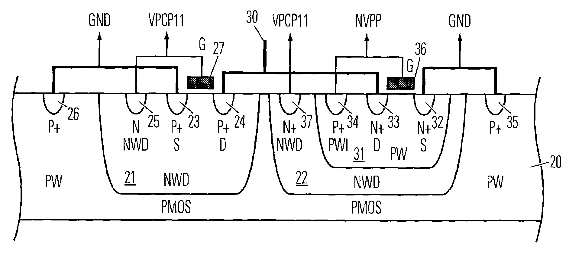
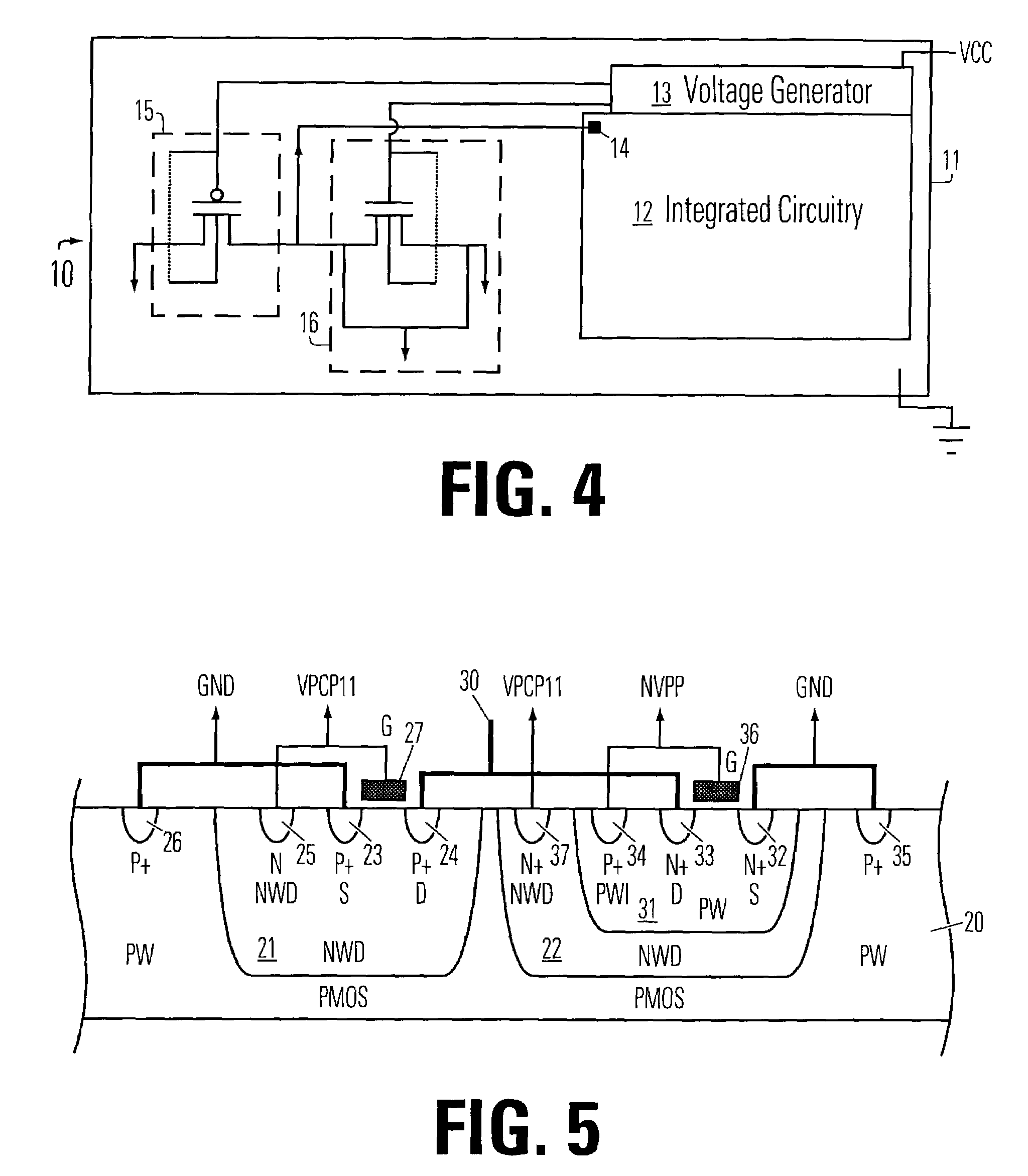
[0027]A detailed description of embodiments of the present invention is provided with reference to FIGS. 4–6. FIG. 4 illustrates an integrated circuit device 10 including a protection circuit according to the present invention. The integrated circuit device includes a device substrate 11. Integrated circuitry 12 on the device substrate performs the “mission” operations for the device 10. The “mission” operations may include providing memory, logic functions, processor functions, or any of a wide variety of functions provided by integrated circuitry.

[0028]A power supply provides a supply voltage VCC and a ground reference for the device substrate 11. Voltage generator circuitry 13 on the device substrate 11 provides operational voltages for the integrated circuit 12, including a lower operating voltage and a higher operating voltage for a node 14.

[0029]The protection device on the device substrate includes a PMOS transistor 15 and an NMOS transistor 16. One of the source / drain termin...


PUM


Abstract

A protection device and a method for manufacturing integrated circuit devices protect against plasma charge damage, and related charge damage during manufacture. The protection device comprises a dynamic threshold, NMOS/PMOS pair having their respective gate terminals coupled to the semiconductor bulk in which the channel regions are formed. With proper metal connection, the structure protects against plasma charge damage on the integrated circuit device during manufacture, and can also be operated to protect against abnormal voltages during operation of the circuit.

Description

BACKGROUND OF THE INVENTION[0001]1. Field of the Invention[0002]The present invention relates to integrated circuit devices and integrated circuit device manufacturing, including manufacturing of non-volatile memory devices, and more particularly to devices and processes for protection of integrated circuitry from plasma damage during manufacture.[0003]2. Description of Related Art[0004]In the manufacturing of integrated circuits, the processes are utilized which utilize activated ions. For example, backend processes including metal etching, photoresist stripping, and deposition of inter-metal dielectrics, involve plasmas which induce charge on the structures being treated. These plasma induced charges may damage underlying structures in the device, including structures critical to device performance. For example, tunnel dielectrics used in flash memory devices, gate dielectrics, and inter-polysilicon dielectrics, can be damaged by plasma induced charge. Furthermore, the charge stor...

Claims


Application Information

Patent Timeline
IPC IPC(8): H01L29/788H01L21/8239H01L21/8246H01L21/8247H01L27/092
CPCH01L27/092H01L27/1052H01L27/11568H01L27/11521H10B99/00H10B43/30H10B41/30
Inventor CHOU, MING HUNGCHEN, TU SHUNHUANG, SMILE
Owner MACRONIX INT CO LTD
Why Eureka
Try Eureka