Configuration memory structure

a memory structure and configuration technology, applied in the field of configuration memory structure, can solve the problems of limiting readback operation, requiring generating another voltage supply, and disturbing the latched value, and achieves fast read and write operation, simple and robust

Active Publication Date: 2007-03-27
MINERAL LASSEN
View PDF13 Cites 60 Cited by
  • Summary
  • Abstract
  • Description
  • Claims
  • Application Information

AI Technical Summary

Benefits of technology

[0020]To obviate the drawbacks of the prior art, one embodiment of the instant invention provides a simple and robust technique of configuration data readback using distributed buffers to ensure fast read and write operation on configuration latches.
[0021]This embodiment of the invention eliminates the second voltage required for read operation.

Problems solved by technology

The limitation of this scheme is that it requires generating another voltage supply for read operation.
The design is sensitive to noise on the column voltage line, which may disturb the latched value.
For high-density devices, the presence of intermediate write buffers on data lines limits the readback operation.

Method used


Image

  • Configuration memory structure
  • Configuration memory structure
  • Configuration memory structure

Examples


Embodiment Construction

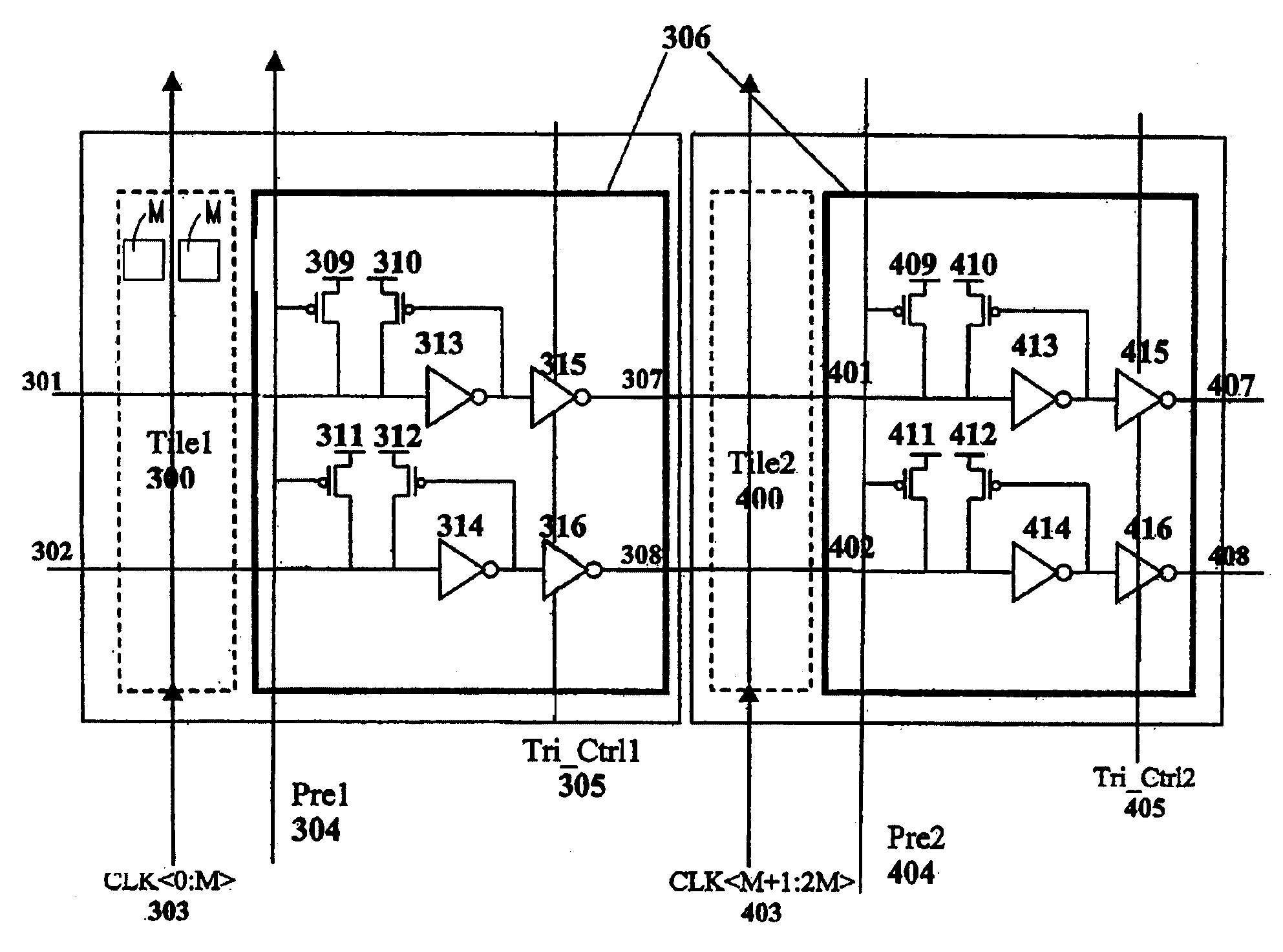
[0039]FIG. 3 represents the schematic of a buffer placed between two tiles of memory cells of a configuration memory array. Each tile includes a sub-array of memory cells (M) as the configuration latches. Preferably each memory cell M is a six-transistor (6T) memory cell that includes two cross-coupled inverters, each with two CMOS transistors, a write transistor, and a read transistor. The tiles (300, 400) also include data lines (301, 401) and inverted data lines (302, 402) connected to the memory cells. CLK303 are column select lines for configuring the memory cells of the tile 300. Similarly CLK403 are column select lines for configuring the memory cells of the tile 400.

[0040]A tristate driver and pre-charge logic 306 is incorporated between every two titles (for e.g., tile 300 and tile 400) for driving the data lines as well as inverted data lines (301, 401, 302, 402) for configuring and precharging the same during configuration data readback. Each tristate driver and pre-charg...


PUM


Abstract

A configuration memory structure includes one or more distributed buffers cascaded together, the output of a first buffer driving an output data line and complementary output data line which terminate at the input of a succeeding buffer. The first buffer includes precharging elements connected between a source and the data line and complementary data line, respectively; data sensing and holding elements connected between respective input and complementary input data lines and the data line and complementary data line, respectively; and tristate elements connected to the outputs of the data sensing and holding elements. This scheme provides fast and reliable configuration and configuration read back, especially for a high density FPGA.

Description

BACKGROUND OF THE INVENTION[0001]1. Field of the Invention[0002]The invention relates to an improved configuration memory structure using one or more distributed buffers.[0003]2. Description of the Related Art[0004]Field programmable gate arrays (FPGAs) are semi-custom devices, which contain a fixed set of gate structures, which can be interconnected in a number of ways to implement a desired logic function by programming the interconnect pattern electrically.[0005]FPGAs generally include an array of programmable logic blocks (PLB). A PLB is also called a configurable logic block (CLB) or a configurable logic element (CLE) or programmable function unit (PFU). Each PLB contains one or more input lines, one or more output lines, one or more latches and one or more look up tables (LUT). The LUT can be programmed to perform various functions including general combinatorial or control logic or a data path between the input and output lines. The LUT thus determines whether the respective ...

Claims


Application Information

Patent Timeline
Patent Type & Authority Patents(United States)
IPC IPC(8): G11C7/10G11C7/00
CPCG11C7/1051G11C7/106G11C7/1078H03K19/17792G11C11/419H03K19/1776H03K19/17776G11C7/1087H03K19/17758
Inventor KHURANA, ANOOPSWAMI, PARVESH
Owner MINERAL LASSEN
Why Eureka
Try Eureka