
Parallel optical subassembly module structure

a technology of parallel optical sub-assembly and module, applied in the direction of optics, optical elements, instruments, etc., can solve the problems of reduced tolerance of fabricating devices and the reliability of production, difficulty in mass production, and unfeasible structure of optical turns, etc., to overcome reflection noise, reduce cross talk, and be more concise and stable

Inactive Publication Date: 2007-04-03
IND TECH RES INST
View PDF13 Cites 4 Cited by
  • Summary
  • Abstract
  • Description
  • Claims
  • Application Information

AI Technical Summary

Benefits of technology

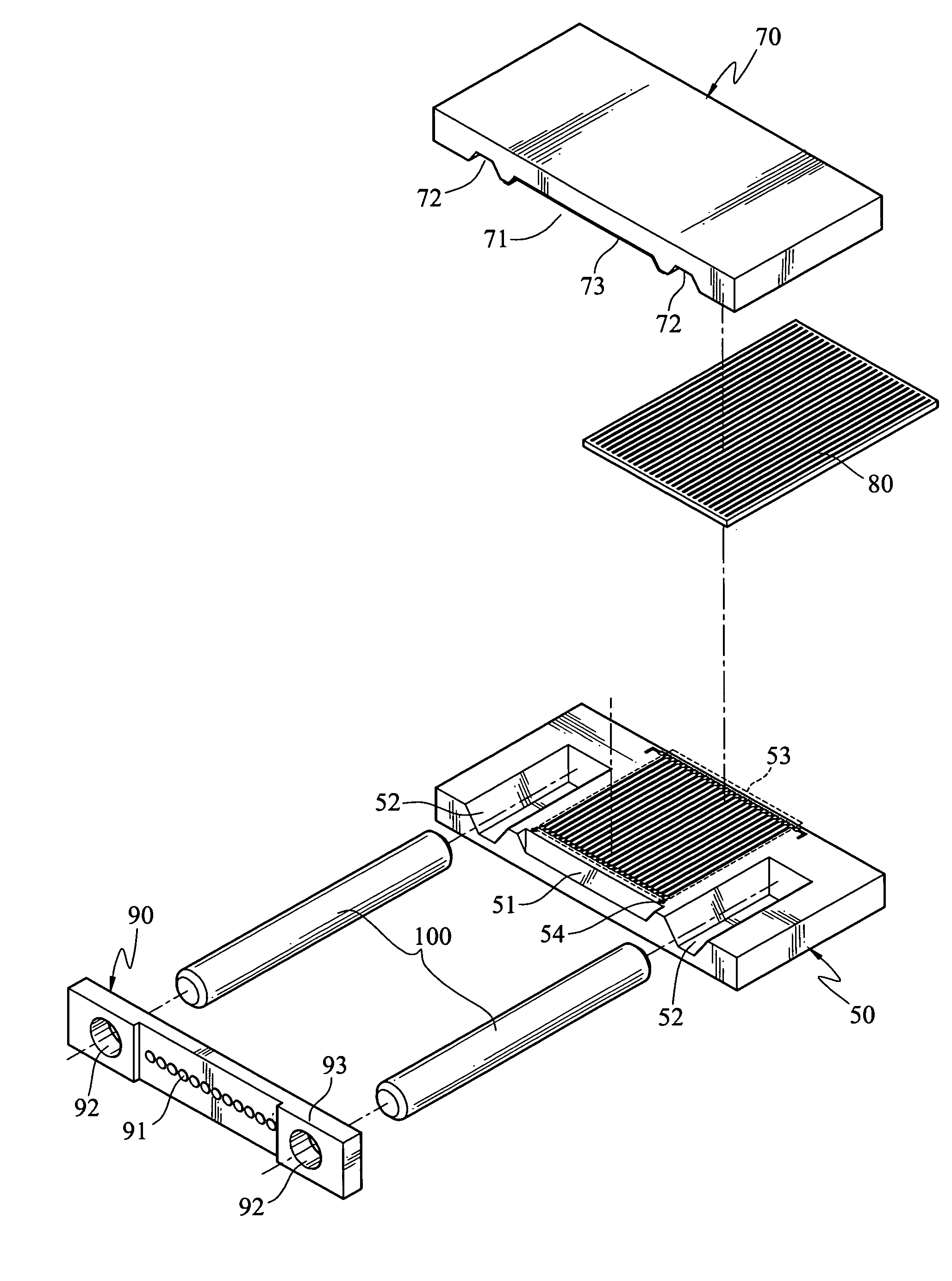
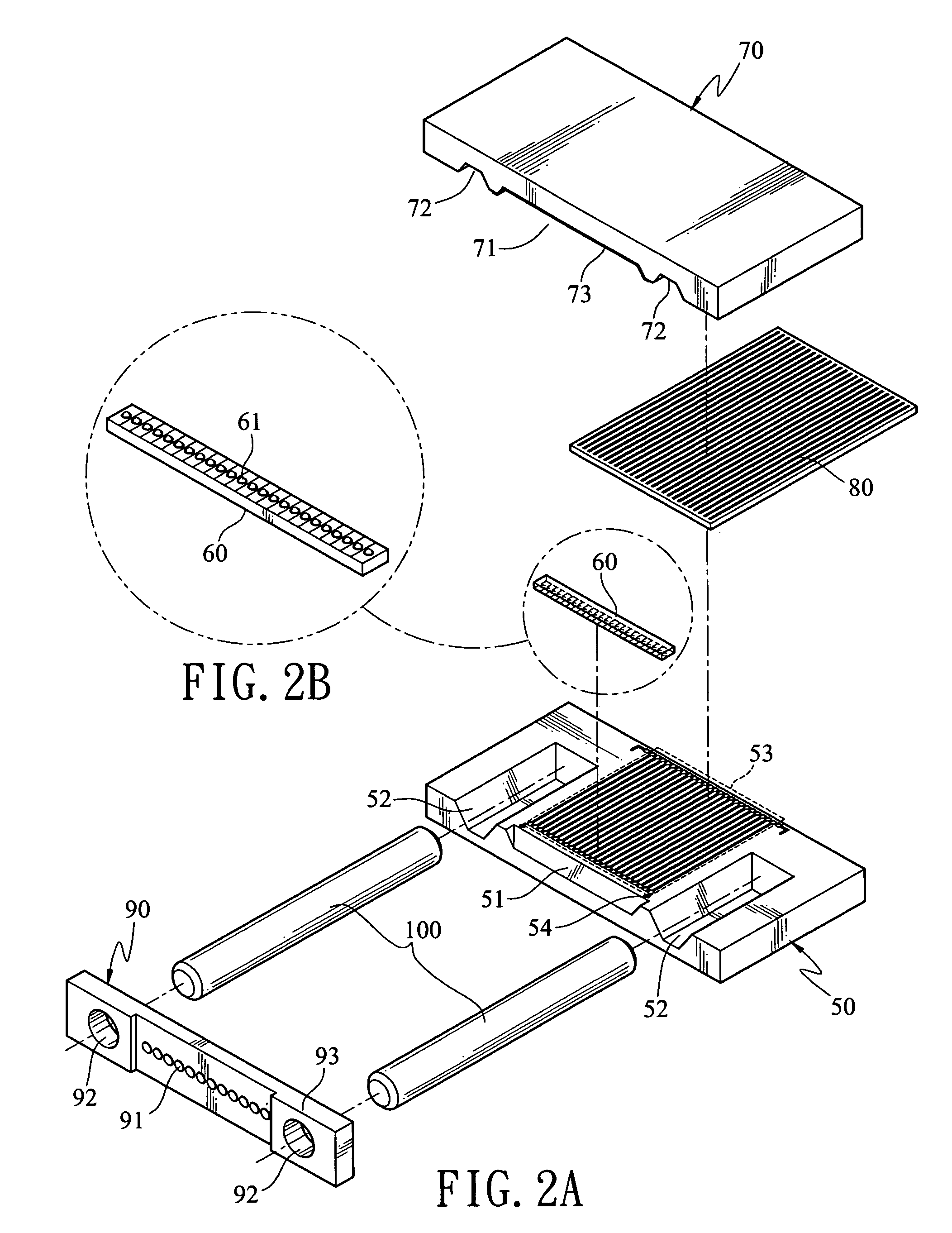
The present invention provides a parallel optical subassembly module structure for transmitting signals in the parallel optical data link system. The structure includes a base, opto-electronic device array, top cover, flexible printed circuit board (FPC), micro-lens array plate, and guide pin. The FPC is used for transmitting electric signals between the base and external circuits. The micro-lens array plate is used for rectifying and outputting optical signals. The guide pin is used for assembling and positioning the module structure and optical connector. The structure is more concise, stable, and effective in transmitting high-frequency signals with wider bandwidth. It can be easily and mass fabricated and has a smaller volume and more stable structure. The invention has various applications in the field of optical data link systems.

Problems solved by technology

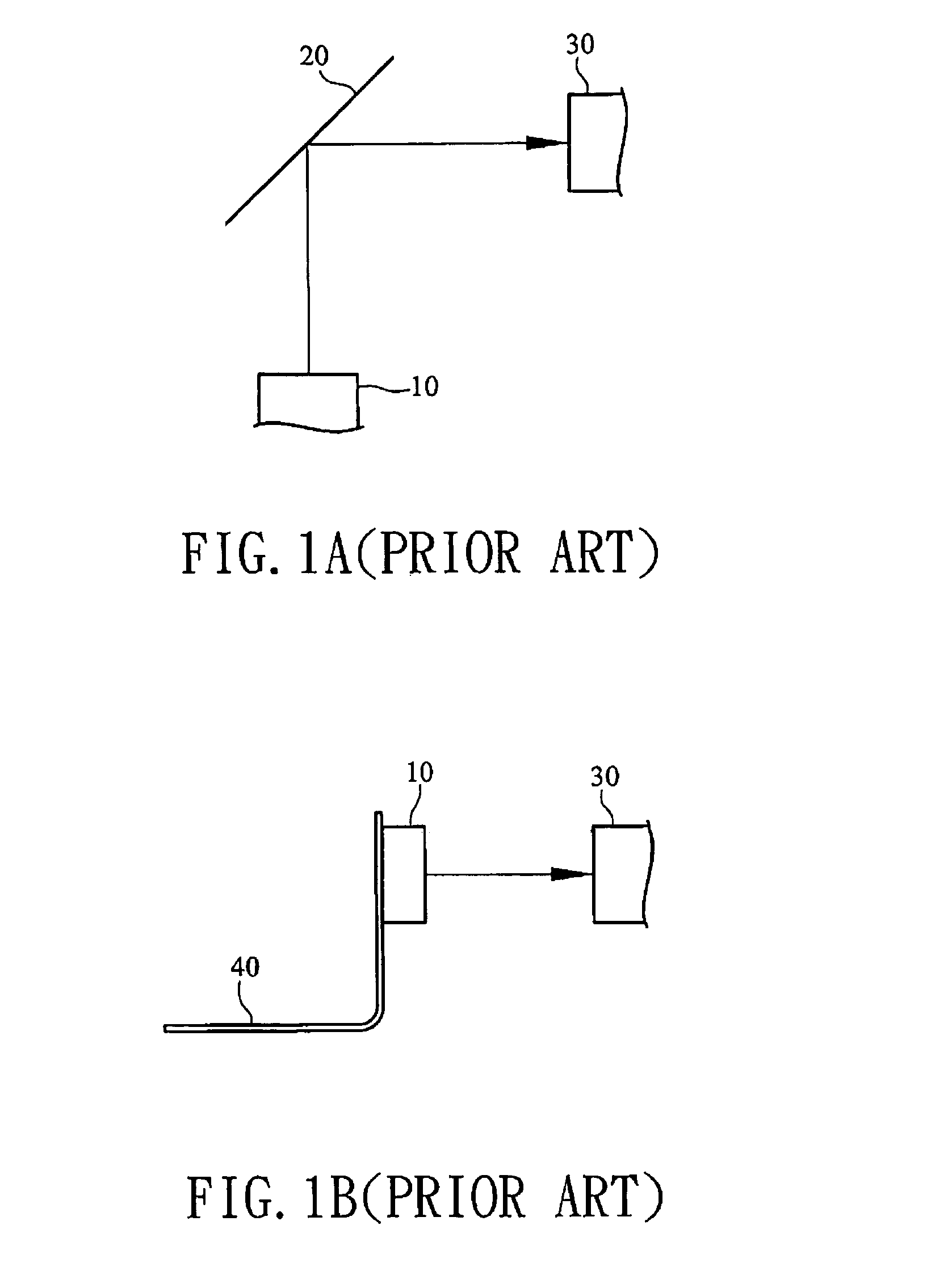
In the structure of an optical turn, many devices are required to achieve an optical turn, and thereby the tolerance of fabricating devices and the reliability of production is reduced.
Besides, the structure of an optical turn is quite unfeasible and has difficulties in mass production.
Furthermore, since some optical devices are made from optical plastic materials with a relatively high coefficient of thermal expansion (CTE) to undergo processes of injection molding, the devices dilate and deform under thermal loading, and the coupling efficiency of devices deteriorate as a result.
Especially in the case of high frequency transmission, there is reflection noise at the bending part of the FPC.
The method of increasing the curvature radius of the bending part of the FPC to diminish negative effects caused by the bending would lengthen the trace of the circuit, and thereby worsen the transmission of high frequency signals.

Method used


Image

  • Parallel optical subassembly module structure
  • Parallel optical subassembly module structure
  • Parallel optical subassembly module structure

Examples


Embodiment Construction

[0041]FIG. 2A and FIG. 2C illustrate an exploded view and a perspective view of a parallel optical subassembly module structure with a preferred embodiment of the present invention respectively, referring to FIG. 2A and FIG. 2C, the module structure, having a base 50, a opto-electronic device array 60, a top cover 70, a flexible printed circuit board (hereafter called as “FPC”) 80, a micro-lens array plate 90, and a guide pin 100, applies to signal transmission of parallel optical data link. FIG. 2B illustrates a bottom view of a opto-electronic device array shown in FIG. 2A

[0042]The module structure can be applied in a optical signal-transmitting part with the opto-electronic device array 60 being a vertical cavity surface emitting laser array (hereafter called as ‘VCSEL array’), or in a optical signal-receiving part with the opto-electronic device array 60 being a PD array. The direction of the optical signal transmission in the module of optical signal-transmitting part is revers...


PUM


Abstract

A parallel optical subassembly module structure comprises an opto-electronic device array, a base with a reflecting slope, and a micro-lens array plate with an inclined plane provided with a specific angle. The optical signal emitted from the opto-electronic device array reflects by the reflecting slope and is incident into the inclined plane of the micro-lens array plate with the specific angle. The inclined plane rectifies the optical signal to output in horizontal direction. Then the optical signal couples with the external fibers through each micro lens of the micro-lens array. The pathway of receiving the optical signal is the same as described above, but in reverse direction.

Description

BACKGROUND OF THE INVENTION[0001]1. Field of Invention[0002]The present invention relates to an optical module structure, and more particularly, to a parallel optical subassembly module structure for a parallel optical data link.[0003]2. Related Art[0004]The parallel optical data link as one of the new methods of transmission has been developed to respond to the shift of fiber communication from a long-distance backbone network to clients.[0005]The so-called parallel optical data link is to transmit parallel optical signals Point-to-Point without doing any parallel / serial switch so as to transmit optical signals in parallel through different fibers at high speed to achieve high bandwidth required by multi-clients in access network.[0006]The parallel optical data link can be practically applied to the board-to-board data link in the back plane of communication apparatus, as well as to the data link between multi-processors and peripheral of high-level servers in LAN (For example: dat...

Claims


Application Information

Patent Timeline
Patent Type & Authority Patents(United States)
IPC IPC(8): G02B6/36G02B6/00G02B6/42H04B10/00
CPCG02B6/4249G02B6/4214G02B6/4292
Inventor KAO, CHIH-TINGKO, CHIH-HSIANGTSAI, BOR-CHENCHU, CHUN-HSUNCHIOU, YII-TAYCHEN, JUNG-TAI
Owner IND TECH RES INST
Learn More