Methodologies for efficient inspection of test structures using electron beam scanning and step and repeat systems

a technology of electron beam scanning and test structure, applied in semiconductor/solid-state device testing/measurement, semiconductor/solid-state device details, instruments, etc., can solve the problems of significant time and throughput penalty, inability to generate high-resolution images with conventional e-beam scanning tools, and inability to rotate and realign the test structur

Active Publication Date: 2007-04-03
KLA TENCOR TECH CORP
View PDF5 Cites 87 Cited by
  • Summary
  • Abstract
  • Description
  • Claims
  • Application Information

AI Technical Summary

Benefits of technology

[0024]These and other features and advantages of the present invention will be presented in more detail in the following spe

Problems solved by technology

The time required to rotate and realign the test structure can be significant.
Because conventional e-beam scanning tools cannot typically generate high resolution images of the defect, the voltage contrast test structure is transferred to a high resolution e-beam step and repeat system after a defect is localized.
The localization of the defect within the failing structure can also be accomplished using a step and repeat system, however, at a significant time and throughput penalty.
Th

Method used


Image

  • Methodologies for efficient inspection of test structures using electron beam scanning and step and repeat systems
  • Methodologies for efficient inspection of test structures using electron beam scanning and step and repeat systems
  • Methodologies for efficient inspection of test structures using electron beam scanning and step and repeat systems

Examples


first embodiment

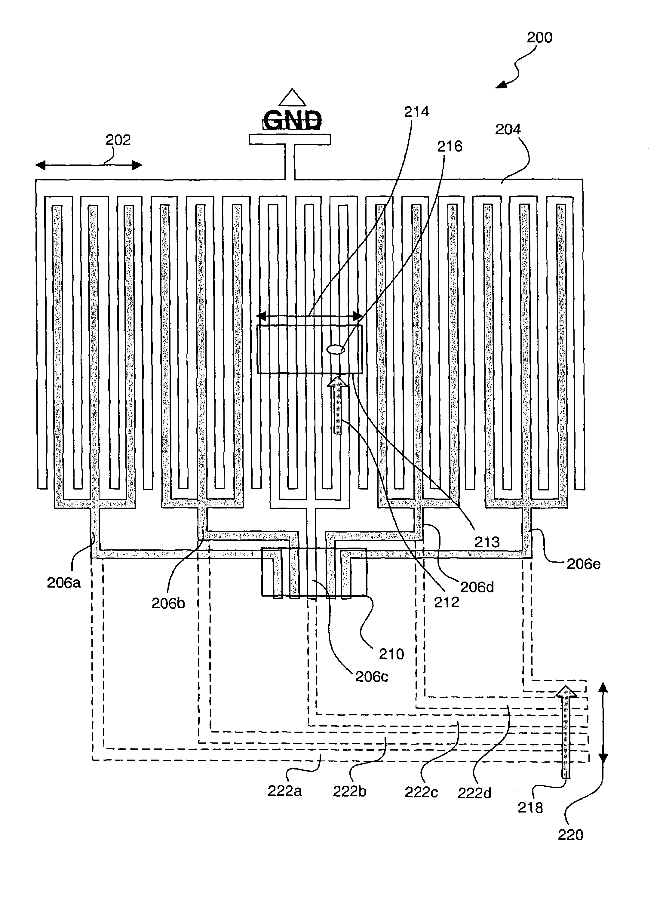
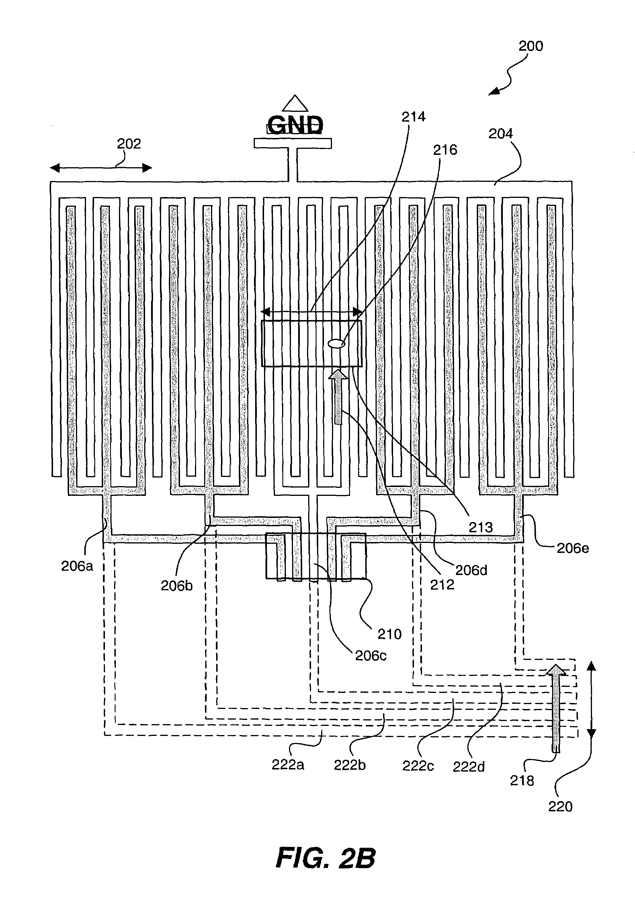
[0042]FIG. 2B is a diagrammatic top view of an example test structure for localizing shorts in accordance with the present invention. As shown, the test structure 200 includes a first conductive substructure 204 having a comb shape. The first substructure 204 is designed to charge to a first voltage potential or brightness level during a voltage contrast inspection. In the illustrated embodiment, the first substructure 204 is coupled to a grounding structure or to a pseudo ground, e.g., the substrate or a relatively large conductive structure (not shown) that will cause the first substructure 204 to charge similarly as if it were coupled to the substrate. A plurality of second conductive substructures having comb shapes 206 are each left floating. The tines of the second substructures 206 are interleaved between the tines of the first substructure 204.

[0043]In the illustrated embodiment, each second substructure 206 has a portion which extends into an area 210 small enough to fit wi...

second embodiment

[0057]The techniques of the present invention may be practiced on other types of test structures, besides the comb type test structure for finding shorts of FIG. 2B. FIG. 5 is a diagrammatic top view representation of a test structure 500 in accordance with the present invention. This test structure 500 is designed to mimic a portion of an SRAM device and is designed to detect the presence of shorts using the techniques described above. Similar to the test structure of FIG. 2B, this SRAM type test structure 500 includes a plurality of substructures 501a through 501e. Each substructure 501 is adjacent to a plurality of other substructures 503 (e.g., 503a and 503b) which are coupled to the substrate through conductive vias (e.g., via 505a), while the substructures 501 remain floating and not coupled with the substrate.

[0058]Alternatively, the adjacent “grounded” substructures 503 may be coupled to a large structure, such as a large probe pad 507, so that the grounded substructures cha...

third embodiment

[0061]A test structure may alternatively be designed to facilitate detection of open type defects. FIG. 6 is a diagrammatic top view representation of a test structure 600 in accordance with the present invention. This test structure 600 includes a plurality of substructures 601a through 601d. Each substructure is designed so that a first end extends into initial field of view area 602, while a second end is coupled to ground.

[0062]An e-beam may initially be scanned over the first ends in field of view area 602 to detect open type defects in substructures 601. In this embodiment, the substructures will appear bright when coupled to ground and dark. However, a substructure's first end (which is opposite the grounded second end) will appear bright when there is an open defect which decouples the first end from ground. As shown, substructure 601a has an open defect 606 and its first end appears dark in field of view area 602. The open defect 606 is found by moving or stepping the e-bea...


PUM


Abstract

Disclosed are techniques for efficiently inspecting defects on voltage contrast test. In one embodiment, methodologies and test structures allow inspection to occur entirely within a charged particle system. In a specific embodiment, a method of localizing and imaging defects in a semiconductor test structure suitable for voltage contrast inspection is disclosed. A charged particle beam based tool is used to determine whether there are any defects present within a voltage contrast test structure. The same charged particle beam based tool is then used to locate defects determined to be present within the voltage contrast test structure. Far each localized defect, the same charged particle beam based tool may then be used to generate a high resolution image of the localized defect whereby the high resolution image can later be used to classify the each defect. In one embodiment, the defect's presence and location are determined without rotating the test structure relative to the charged particle beam.

Description

CROSS REFERENCE TO RELATED APPLICATIONS[0001]This application claims priority of U.S. Provisional Patent Application No. 60 / 463,544 filed 16 Apr. 2003, which application is incorporated herein by reference in its entirety for all purposes.BACKGROUND OF THE INVENTION[0002]This invention relates to methods and apparatus for detecting electrical defects in a semiconductor device or test structure. Additionally, it relates to generating an image of each identified defect for use in various defects analysis procedures, such as automatic defect classification.[0003]Several different types of systems and techniques exist for identifying electrical defects, such as shorts and opens, on a semiconductor device or test structure. Commonly, test structures include probe pads that can be electrically probed to detect the existence of opens or shorts within such test structure. Another type of test structure is referred to as a voltage contrast type test structure. Electrical defects can be detec...

Claims


Application Information

Patent Timeline
IPC IPC(8): H01L21/66G01R31/307G01R31/316H01L23/544
CPCG01R31/307H01L22/34
Inventor VERMA, GAURAVWEINER, KURT H.
Owner KLA TENCOR TECH CORP
Why Eureka
Try Eureka