Stacked electrical resistor pad for optical fiber attachment

a technology of electrical resistor pads and optical fibers, which is applied in the direction of resistor details, optical elements, instruments, etc., can solve the problems of difficult laser soldering, inefficient heat transfer of laser beams, and difficult laser soldering with 80au-20sn, and achieve low resistance and high resistance

Inactive Publication Date: 2007-04-03
EMCORE INC
View PDF55 Cites 51 Cited by
  • Summary
  • Abstract
  • Description
  • Claims
  • Application Information

AI Technical Summary

Benefits of technology

[0007]In one aspect of the present invention, an electrical resistor structure overlies a substrate and comprises a composite resistor having a first resistor of relatively low resistance and a second resistor of relatively high resistance overlying the first resistor. First and second electrodes make contact with the composite resistor at spaced locations, and a bond pad, overlies the second resistor at a position between the electrodes.

Problems solved by technology

However, soldering with 80Au-20Sn is challenging.
Laser soldering suffers from the limitation that because solder metal reflects laser light, focusing the laser beam directly on solder does not transfer heat efficiently.
Also, laser soldering requires an optical path, which is often difficult in many-layered or complicated optical devices.
An often-encountered problem is mechanical failures (cracking or delamination) of the heating electric resist layer.
Particularly, thick-film resistors are more vulnerable than thin-film resistors, because thick-film resistors contain more inherent defects.
Other non-trivial issues in resist heating are the structure design of resistor pad and the parameter selection of the heating process.

Method used


Image

  • Stacked electrical resistor pad for optical fiber attachment
  • Stacked electrical resistor pad for optical fiber attachment
  • Stacked electrical resistor pad for optical fiber attachment

Examples


Embodiment Construction

Structure

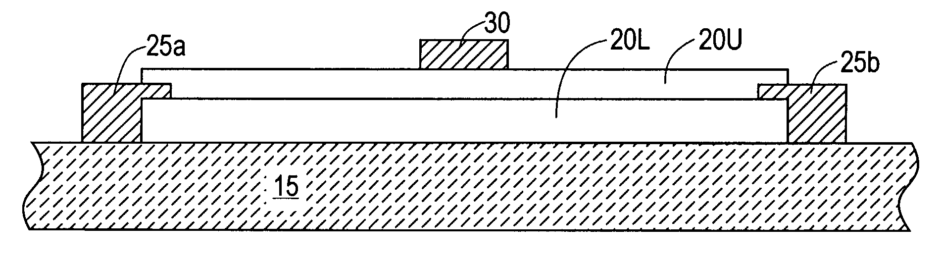
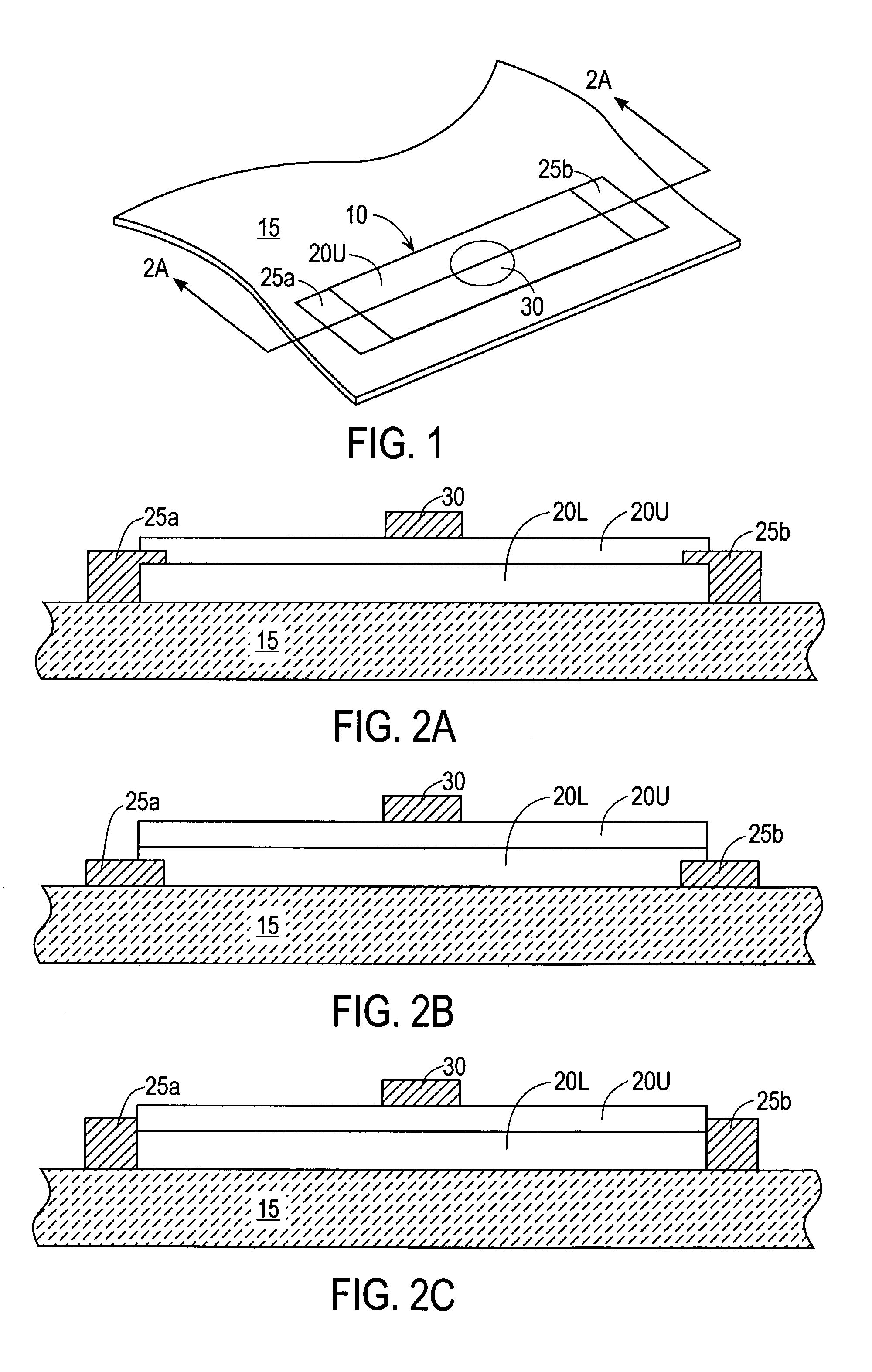
[0015]FIG. 1 is a perspective view of a stacked electrical resistor structure 10 according to an embodiment of the present invention. FIG. 2A is a cross-sectional view of resistor structure 10 taken along line 2A—2A in FIG. 1. The figures are drawn with the resistor structure extending in a nominally horizontal plane, and for purposes of description, that orientation will be used, it being recognized that when the resistor structure is ultimately in a larger assembly, the assembly, and hence the resistor structure, may be in any orientation.

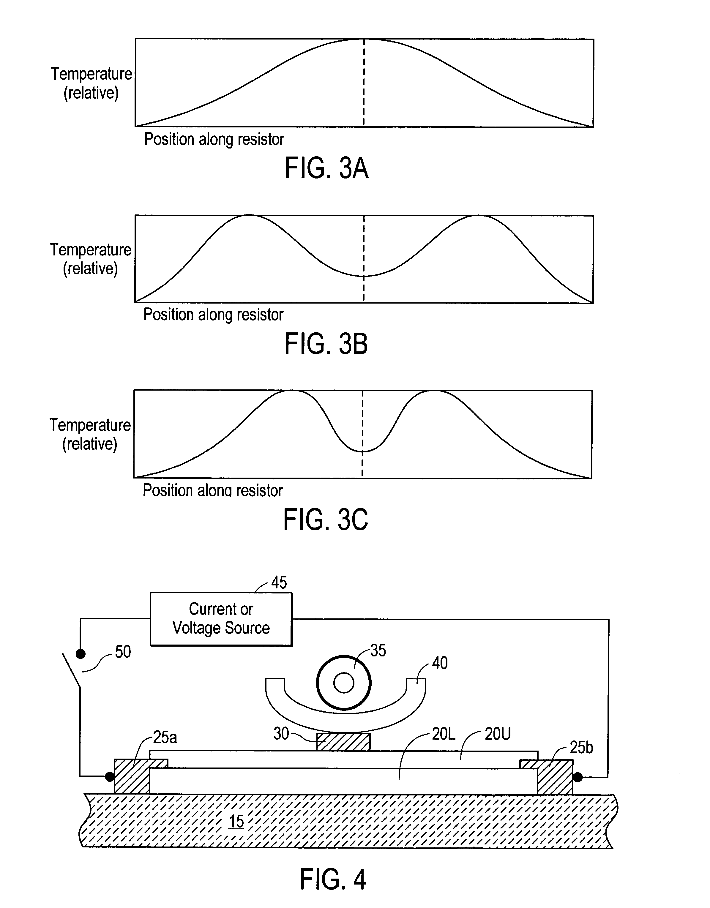
[0016]Resistor structure 10 overlies a non-conductive substrate 15, and has upper and lower electrically resistive layers 20U and 20L, which are sometimes referred to as the upper and lower resistors. Lower resistor 20L is closest to the substrate, and is not visible in FIG. 1 (being hidden under upper resistor 20U). The resistor structure further includes a pair of metal electrodes 25a and 25b at opposite ends, and a metal bond pad 30 o...


PUM


Abstract

An electrical resistor structure overlies a substrate and comprises a composite resistor having a first resistor of relatively low resistance and a second resistor of relatively high resistance overlying the first resistor. First and second electrodes make contact with the composite resistor at spaced locations, and a bond pad overlies the second resistor at a position between the electrodes. A metallized fiber is soldered a to a metal bond pad by providing a stacked resistor structure beneath the bond pad, disposing a solder preform over the bond pad, disposing the metallized fiber over the bond pad, and flowing a current through the stacked resistor structure. The stacked resistor structure, when subjected to a current flowing generally along a first axis, is characterized by a temperature profile that has first and second peaks on either side of the bond pad. The fiber is disposed along a second axis in the region of the bond pad where the second axis is at a non-zero angle (possibly, but not necessarily a right angle) with respect to the first axis.

Description

BACKGROUND OF THE INVENTION[0001]This application relates generally to fiber optic device manufacture and more specifically to techniques for efficiently soldering components such as metallized fiber to a metallized region on a substrate.[0002]In the fabrication of fiber optic modules and the like, it is necessary to bond optical fibers to substrates, and it is common to solder a metallized fiber to a metallized region on a substrate to accomplish such bonding. A gold-tin (Au—Sn) alloy solder such as 80Au-20Sn is often used due to a number of desirable properties. For example, soldering with 80Au-20Sn may be fluxless, thereby eliminating the damage to optical properties due to flux residue. Also, 80Au-20Sn solder is the highest in mechanical strength and creep resistance among soft solders, so that optical alignment can be maintained over a long period. Further, pull test results from fiber metallizing vendors suggest that the interface between Au—Sn solder and metallized (with Ni / A...

Claims


Application Information

Patent Timeline
Patent Type & Authority Patents(United States)
IPC IPC(8): H01L29/00
CPCG02B6/4238
Inventor MEI, ZEQUNBJORN, RICHARD D.KUSNADI, FRANSMAJOR, JOHN CAMERON
Owner EMCORE INC
Why Eureka
Try Eureka