
System and method for classifying, detecting, and counting micropipes

a micropipe and counting technology, applied in the field of optical surface analyzers, can solve the problems of loss of yield in the device manufacturing process, defects or dislocations, and defects in the atomic lattice, and achieve the effect of accurate determination of micropipe defects and accurate identification

Active Publication Date: 2007-04-10
KLA TENCOR TECH CORP
View PDF76 Cites 18 Cited by
  • Summary
  • Abstract
  • Description
  • Claims
  • Application Information

AI Technical Summary

Benefits of technology

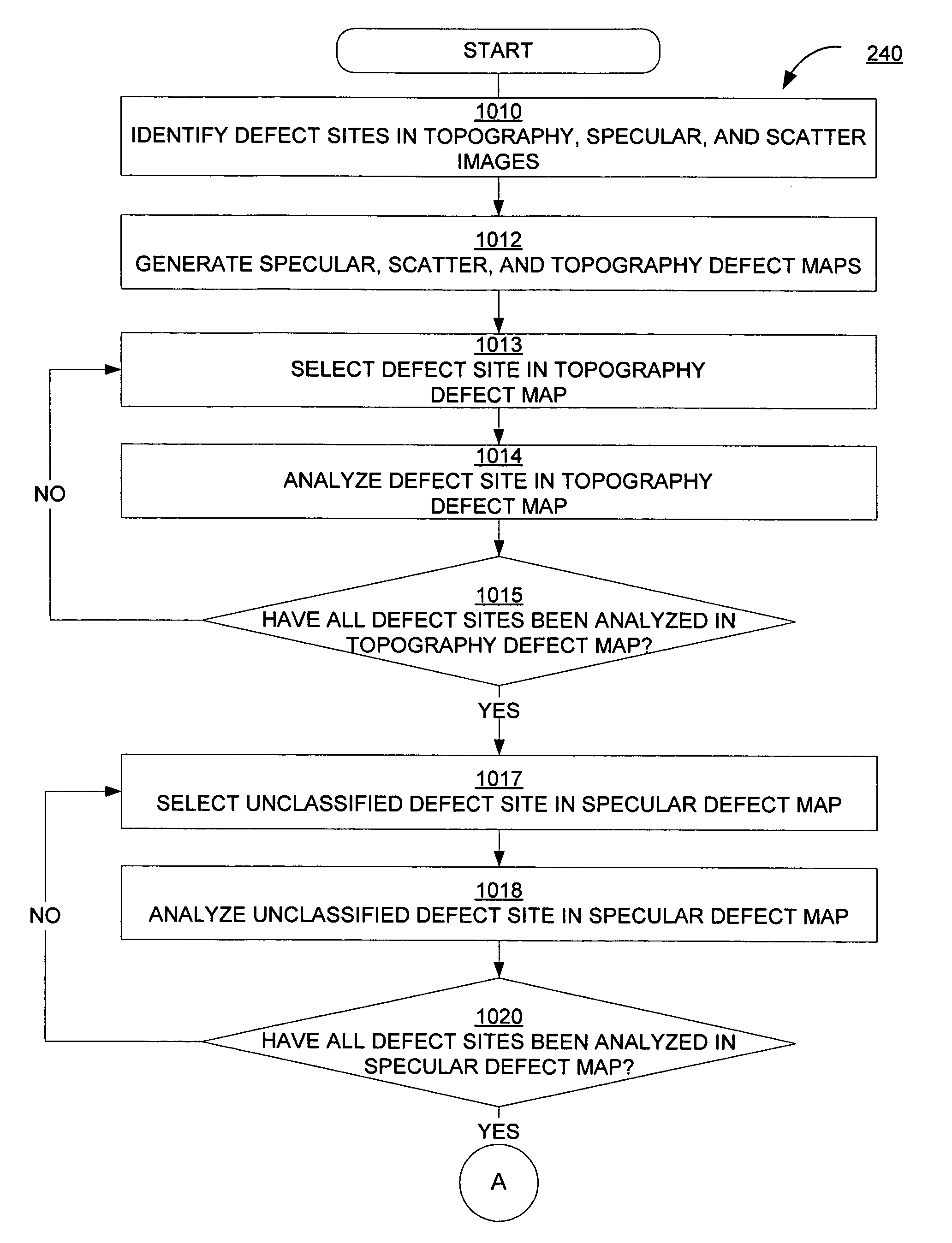
[0008]The present invention overcomes the limitations of the conventional systems by enabling the detection, classification, and counting of micropipes contained within a SiC wafer in a fully automated and non-invasive manner through the use of an optical surface analyzer (OSA) and a unique data processing algorithm that accurately identifies micropipe defects. Within the structure of the data processing algorithm of the present invention, information regarding the size of a defect, the shape of the defect, the area of a defect, and the presence of a tail within the defect signature is produced in order to make an accurate determination regarding the presence of a micropipe.

Problems solved by technology

During the production of these wafers, the crystalline structure is subjected to various internal and external stresses that can cause the growth of defects, or dislocations, within the atomic lattice.
The presence of a high density of micropipes within a wafer will result in a loss of yield in the device manufacturing process.
This process is both destructive to the sample, due to the harsh nature of the KOH etch, and is time consuming, because of the large amount of data that is generated for accurate inspection of the micropipe sites.
Etching micropipes with a KOH solution widens the opening of the micropipe, which does allow for easier inspection; however, the wafer is destroyed in the process, which in turn, drives up the cost of manufacture.
Also, automated inspection of the micropipe sites has been confined to a manual process where a series of JPEG or BITMAP images of the wafer obtained via a cross-polarization technique are stitched together and analyzed for micropipes.
Again, the current techniques are both destructive to the sample and inspect the samples less efficiently, thus translating to a high cost for manufacture.
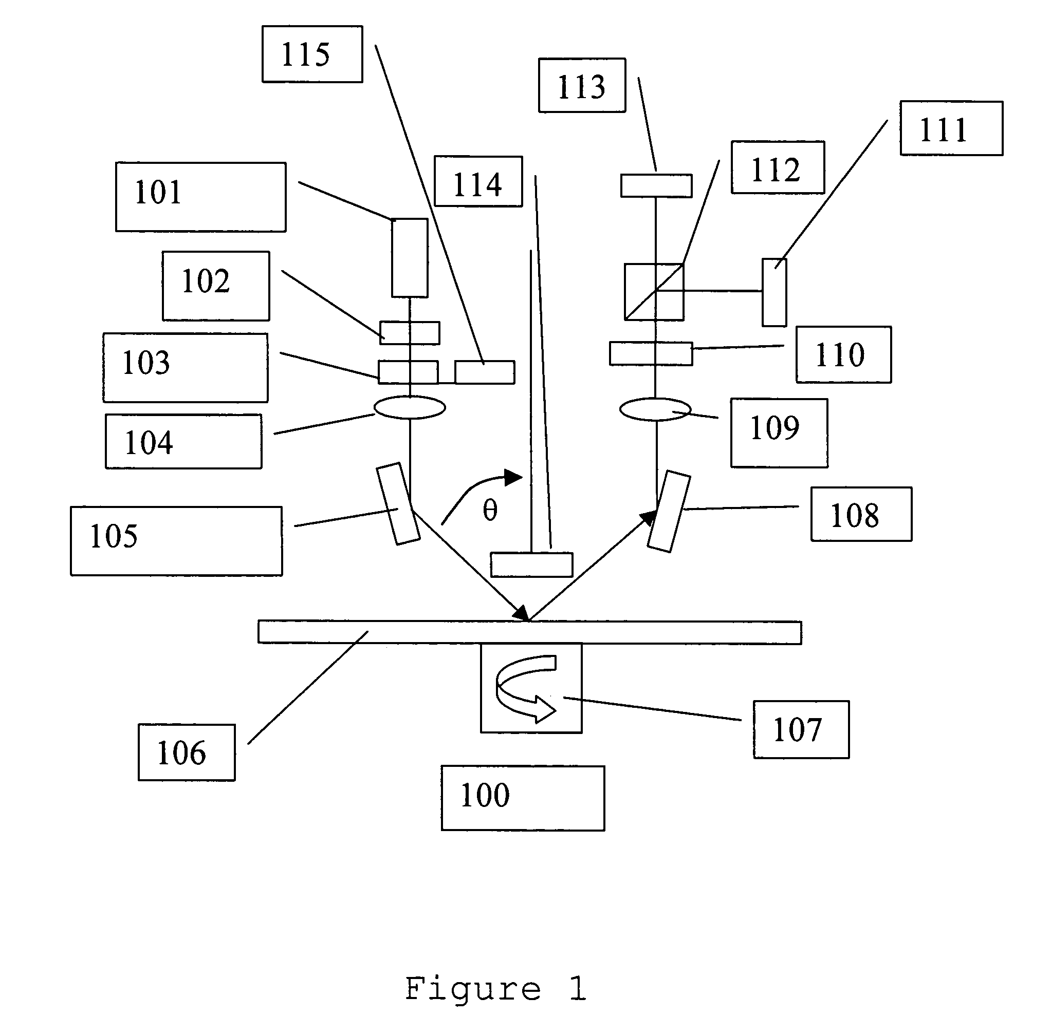
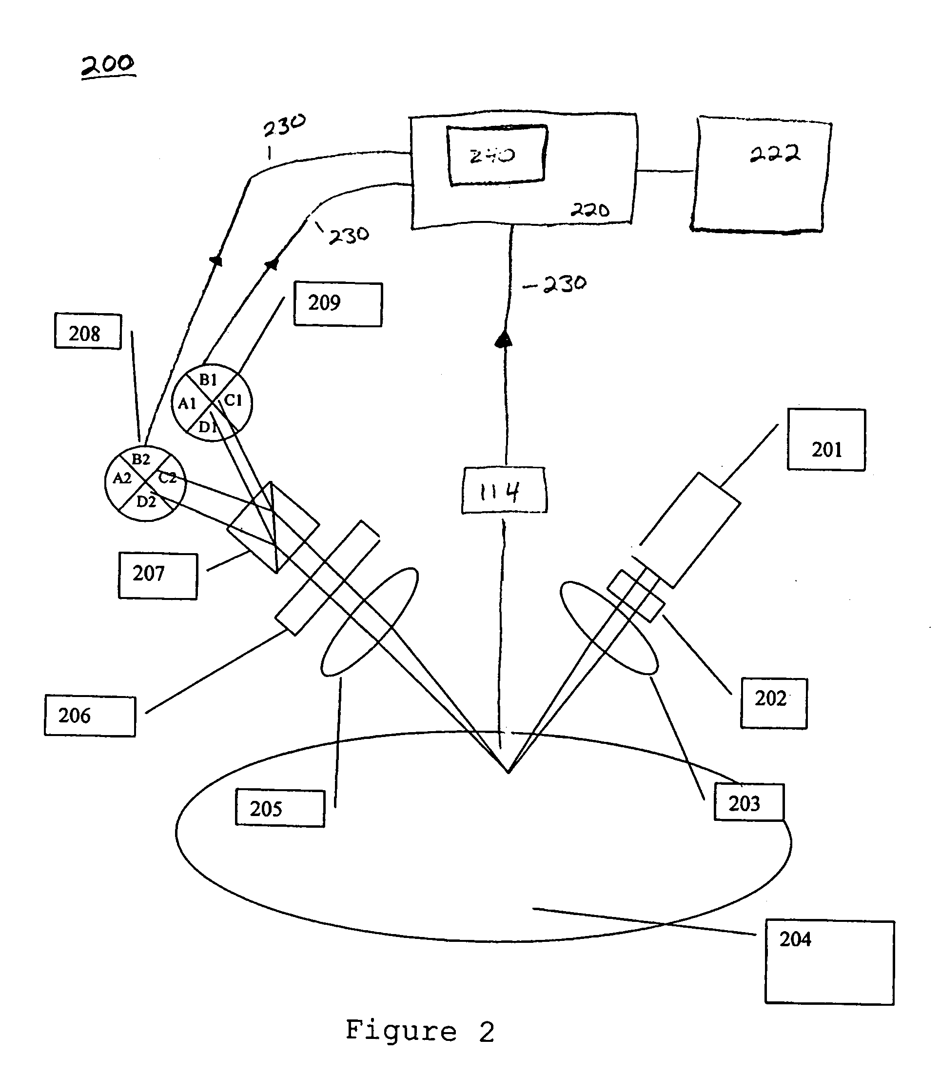
Conventional surface analysis systems are not provided with automated capabilities to collect surface data and cannot avoid contamination of the reflected signals from the top surface of a transparent wafer by reflected light from the back side of a transparent wafer.

Method used


Image

  • System and method for classifying, detecting, and counting micropipes
  • System and method for classifying, detecting, and counting micropipes
  • System and method for classifying, detecting, and counting micropipes

Examples


Embodiment Construction

[0025]A preferred embodiment of the present invention is now described with reference to the figures where like reference numbers indicate identical or functionally similar elements. Also in the figures, the left most digits of each reference number corresponds to the figure in which the reference number is first used.

[0026]Reference in the specification to “one embodiment” or to “an embodiment” means that a particular feature, structure, or characteristic described in connection with the embodiments is included in at least one embodiment of the invention. The appearances of the phrase “in one embodiment” in various places in the specification are not necessarily all referring to the same embodiment.

[0027]Some portions of the detailed description that follows are presented in terms of algorithms and symbolic representations of operations on data bits within a computer memory. These algorithmic descriptions and representations are the means used by those skilled in the data processin...


PUM


Abstract

An automated, non-invasive method for classifying, detecting, and counting micropipes contained within silicon wafers, and generally any assortment of transparent wafers. Classifying, detecting, and counting micropipes takes place through the use of a data processing algorithm that incorporates information regarding: defect size; pit signature; area of pit signature when comparing a topography, specular, or scatter images; and detecting a tail within the standard pit signature. The method of the present invention teaches the development of a topography defect map, specular defect map, and scatter defect map for a complete analysis of the surface of a particular transparent wafer. Conventional detection, classification, and counting of micropipes involve characterization of micropipes in a manual fashion and rely upon an extremely invasive form of sample preparation. The method disclosed in the present invention is completely automated and non-invasive with regards to the treatment of the transparent wafer to be analyzed.

Description

BACKGROUND OF THE INVENTION[0001]1. Field of the Invention[0002]The present invention generally relates to the field of optical surface analyzers and more specifically to the characterization and mapping of micropipes (screw dislocations) on grown wafers.[0003]2. Description of Background Art[0004]Silicon carbide (SiC) wafers are used in a variety of industries such as power devices for automobiles and high frequency communication devices. During the production of these wafers, the crystalline structure is subjected to various internal and external stresses that can cause the growth of defects, or dislocations, within the atomic lattice. A screw dislocation is a common dislocation that transforms successive atomic planes within a crystalline lattice into the shape of a helix. Once a screw dislocation propagates through the bulk of a sample during the wafer growth process, a micropipe is formed. The presence of a high density of micropipes within a wafer will result in a loss of yiel...

Claims


Application Information

Patent Timeline
IPC IPC(8): C30B25/12
CPCC30B25/16C30B29/36
Inventor VELIDANDLA, VAMSI
Owner KLA TENCOR TECH CORP
Learn More