Asynchronous control of memory self test
- Summary
- Abstract
- Description
- Claims
- Application Information
AI Technical Summary
Benefits of technology
Problems solved by technology
Method used
Image

Examples
Embodiment Construction
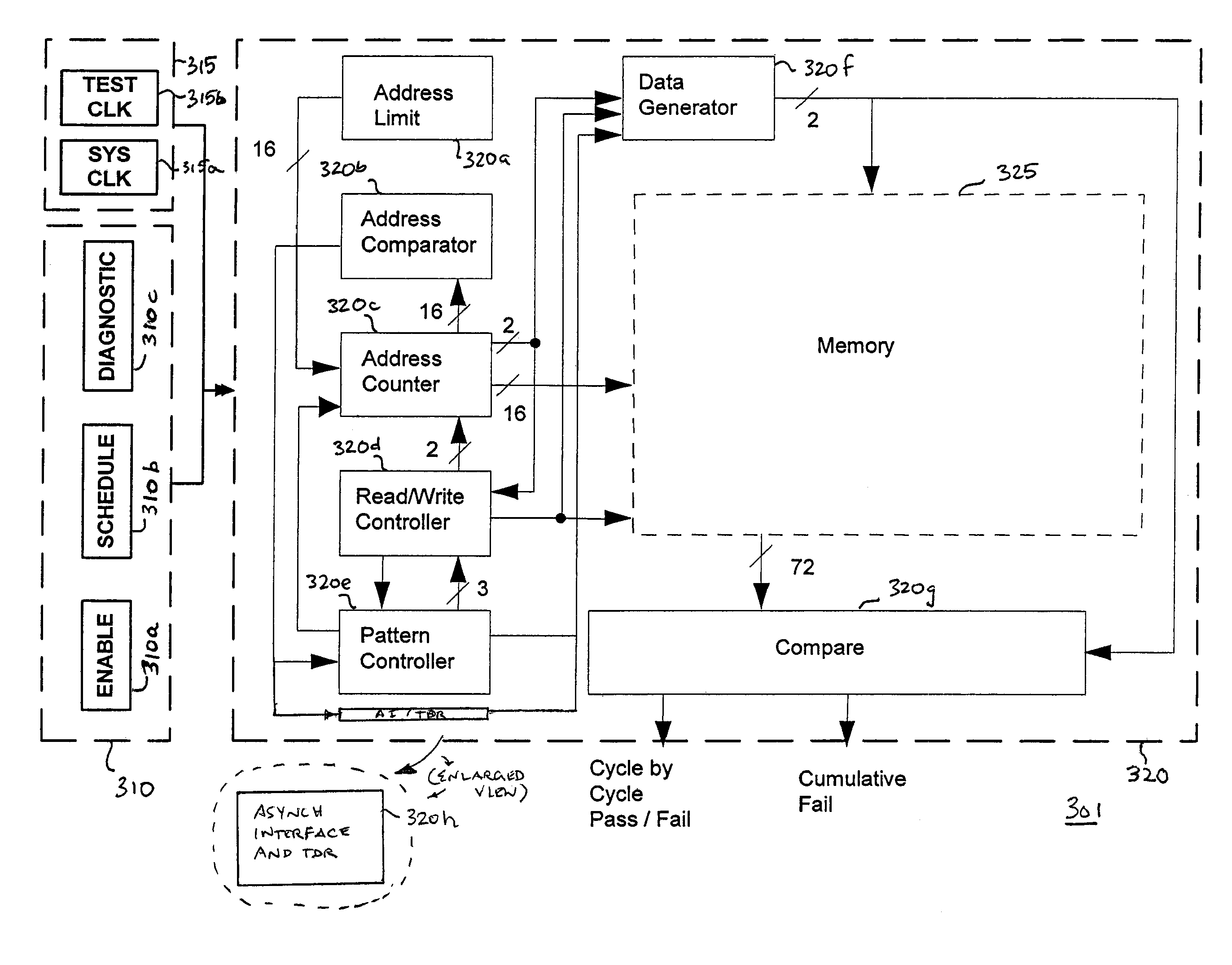
[0023]The Figures (“FIG.”) and the following description relate to preferred embodiments of the present invention by way of illustration only. Embodiments of the present include structures and processes in an integrated circuit chip built-in self-test (“BIST”) environment for testing memories of differing (or varying) types with a universal BIST controller. The present invention may be used with any BIST environment, including IEEE 1149.1 JTAG boundary scans.
Overview of a BIST Environment
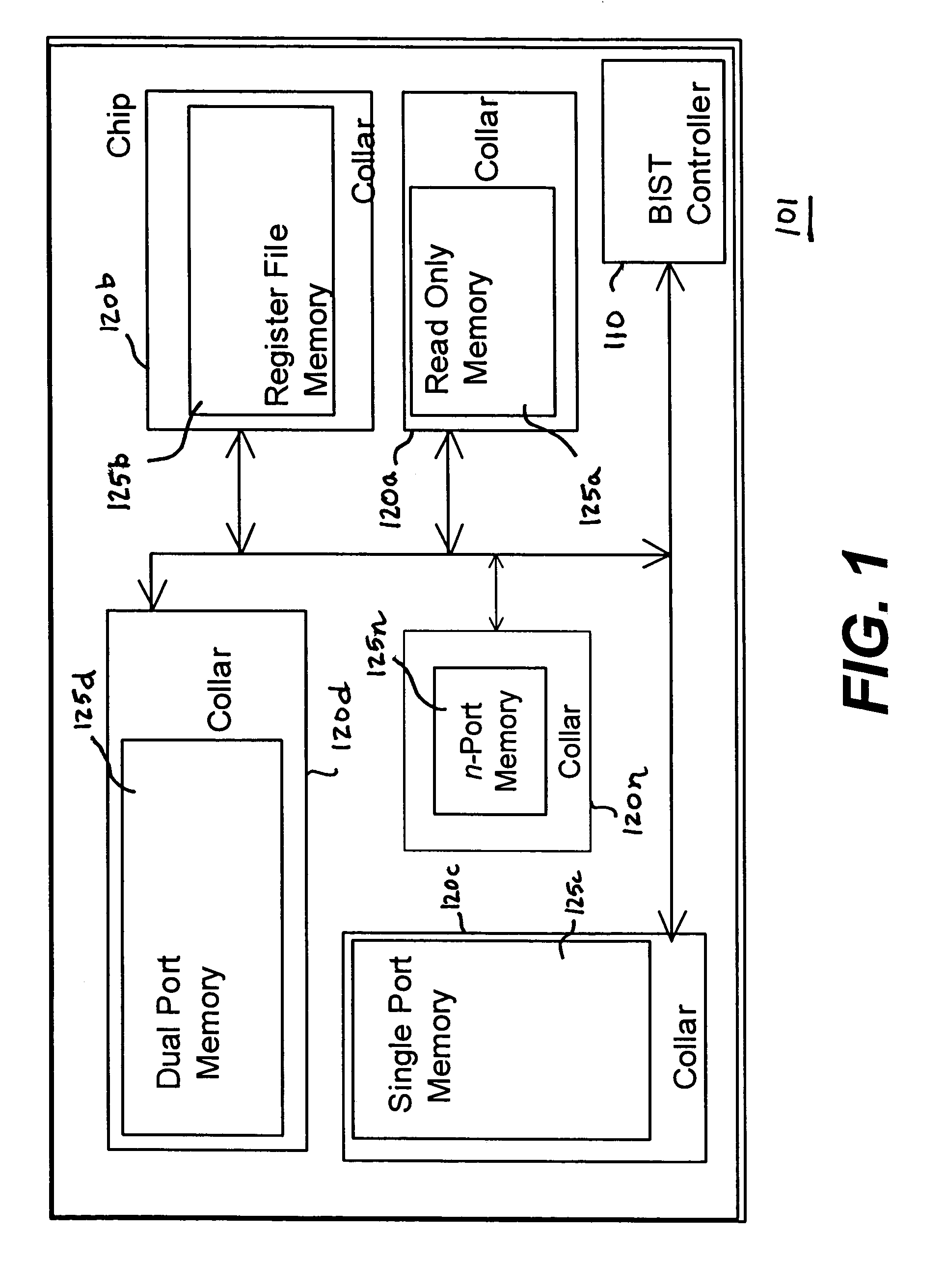
[0024]FIG. 1 illustrates an embodiment of an integrated circuit chip BIST environment 101 including a universal BIST controller 10 and multiple memory types 125a–n (generally 125), each with associated collar 120a–n (generally 120), where n is any integer value, in accordance with the present invention. The BIST environment 101 includes one instance of the universal BIST controller 110 that bi-directionally communicates with and functions with any memory type in the BIST environment 101 through the ...
PUM
 Abstract
Description
Claims
Application Information
 - Generate Ideas
- Intellectual Property
- Life Sciences
- Materials
- Tech Scout
- Unparalleled Data Quality
- Higher Quality Content
- 60% Fewer Hallucinations
Browse by: Latest US Patents, China's latest patents, Technical Efficacy Thesaurus, Application Domain, Technology Topic, Popular Technical Reports.
© 2025 PatSnap. All rights reserved.Legal|Privacy policy|Modern Slavery Act Transparency Statement|Sitemap|About US| Contact US: help@patsnap.com