

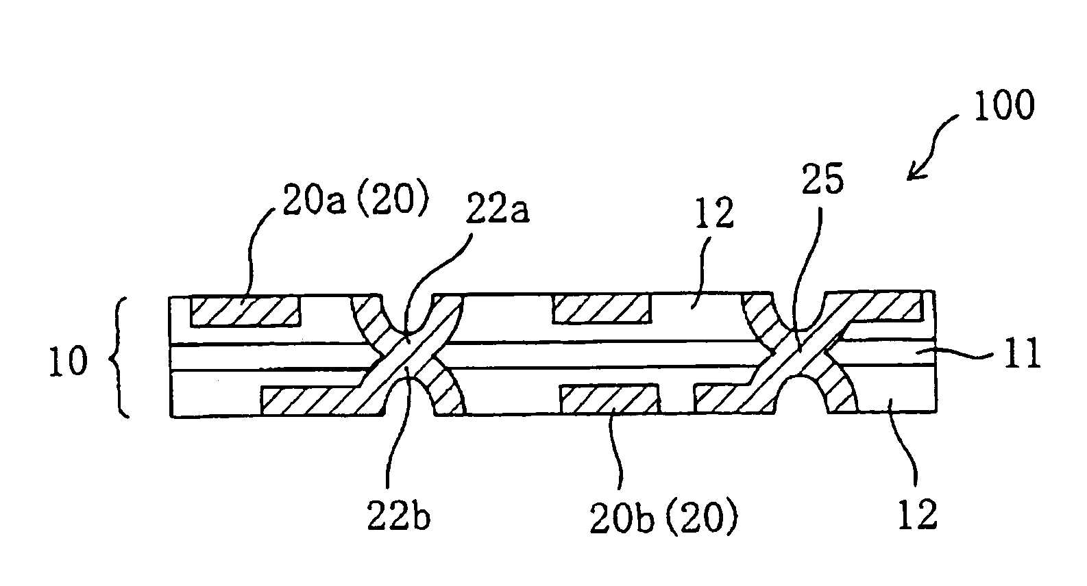
Flexible substrate having interlaminar junctions, and process for producing the same
a technology of interlaminar junctions and flexible substrates, which is applied in the direction of printed element electric connection formation, non-printed electric component association, instruments, etc., can solve the problems of affecting the production process, affecting the flexing life of the substrate, so as to improve the production and mass production. , the effect of preventing a discordance of an impedance and easy holding of the sheet member
- Summary
- Abstract
- Description
- Claims
- Application Information
AI Technical Summary
Benefits of technology
Problems solved by technology
Method used
Image

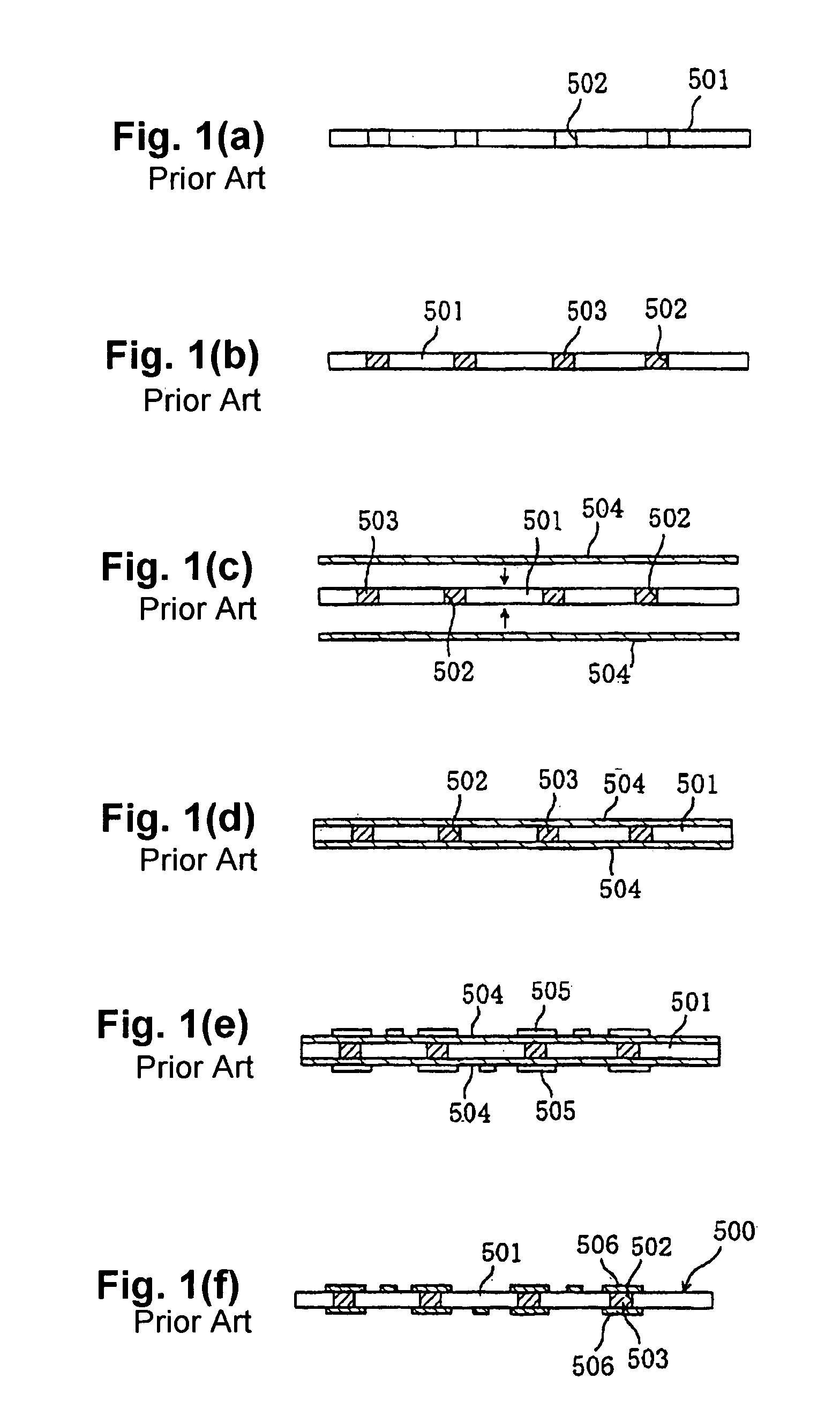
Examples
example 1
[0184](Film Material)
[0185]A film (organic film) used in this example is shown in Table 1.
[0186]
TABLE 1No.FILMNAME OF COMMODITY (MANUFACTURER)1aARAMID┌MICTRON┘(TORAY Co., Ltd.)1bARAMID┌ARAMICA┘(TEIJIN ADVANCED FILMCo., Ltd.)1cPI┌KAPTON┘(DU PONT-TORAY Co., Ltd.)1dPI┌UPILEX┘(UBE INDUSTRIES Co. Ltd.)1ePEN┌TEONEX┘(TEIJIN-DU PONT FILM Co. Ltd.)1fPET┌TETRON┘(TEIJIN-DU PONT FILM Co. Ltd.)1gPPS┌TORELINA┘(TORAY Co., Ltd)1hPA┌HARDEN┘(TOYOBO Co., Ltd)1iPC┌PANLITE┘(TEIJIN CHEMICALS Co., Ltd)1jPES┌SUMILITE FS-1300┘(SUMITOMO BAKELITECo., Ltd)1kPEI┌SUPERIO UT┘(MITSUBISHI PLASTICS, Inc.)1lPPE┌DIANIUM┘(MITSUBISHI PLASTICS, Inc.)1mPEEK┌SUMILITE FS-1100C┘(SUMITOMOBAKELITE Co., Ltd)
[0187](Preparation of the Substrate Used for Measuring Flexing Life)
[0188]By applying an epoxy-base thermosetting resin layer to both surfaces of the film with a roll coater process, insulating resin layers were formed. Subsequently, wiring patterns were embedded into the insulating resin layers.
[0189]Prior to embedding of t...
example 2
[0197](Preparation of a Substrate Used for Measuring Flexing Life)
[0198]In this example, by using a method similar to that of above example (1), various types of sample substrates were prepared in such a manner that a ratio of insulating resin layer thickness / film thickness is diversely changed. Specifications of prepared substrates are shown in the following Table 3.
[0199]
TABLE 3MODULUS OFTHICKNESS(μm)ELASTICITY (GPa)INSULATINGINSULATINGINSULATINGRESIN LAYERORGANICWIRINGRESIN LAYER (ON ONERESINTHICKNESS / No.FILMPATTERNSURFACE OF FILM)FILMSUBSTRATELAYERFILMFILM THICKNESS2aARAMID3124280.8133.02bARAMID3116.528.50.8131.72cARAMID39.59280.8131.12dARAMID3812280.8130.72eARAMID3616280.8130.42fARAMID369210.8130.72gARAMID3129330.8131.3
[0200](Test Condition)
[0201]All of the films used in this example were aramid films (“MICTRON” manufactured by TORAY Co., Ltd.) Sample substrates 2a to 2e were approximately same in thickness thereof, and sample substrates 2c, 2f, and 2g were same in thickness of...
example 3
[0204]In this example, an effect of a pressure-joint performed in a production process of the present invention was confirmed. And also, an effect of an application of the ultrasonic wave to interlaminar junctions was confirmed.
[0205](Preparation of a Substrate Used for Example (3))
[0206]As with example (1), a film on both surfaces of which insulating resin layers were formed was prepared, and also two carrier sheets (i.e. copper foils that were respectively 70 μm in thickness) in which wiring patterns were formed were prepared. The film used in example (3) was aramid film (“MICTRON” manufactured by TORAY Co., Ltd.) being 4 μm in thickness. Each of insulating resin layers formed on both surfaces of the film was 10 μm in thickness. Each of the wiring patterns on the carrier sheets was formed by performance of an electroplating technique in such a manner that a thickness of the wiring pattern was 9 μm. Subsequently, each of the carrier sheets on which the wiring patterns were prelimin...
PUM
 Abstract
Description
Claims
Application Information