

Increased capacity leadframe and semiconductor package using the same
a technology of semiconductor packaging and leadframe, which is applied in the manufacture of cables/conductor devices, solid-state devices, semiconductor devices, etc., can solve the problems of excessive narrowing of lead pitch, physical limitations of narrowing lead pitch during the manufacture of leadframes, and susceptibility to solder shorting between, so as to achieve the formation of lead and die paddle of leadframes. , the effect of lead formation
- Summary
- Abstract
- Description
- Claims
- Application Information
AI Technical Summary
Benefits of technology
Problems solved by technology
Method used
Image

Examples
first embodiment
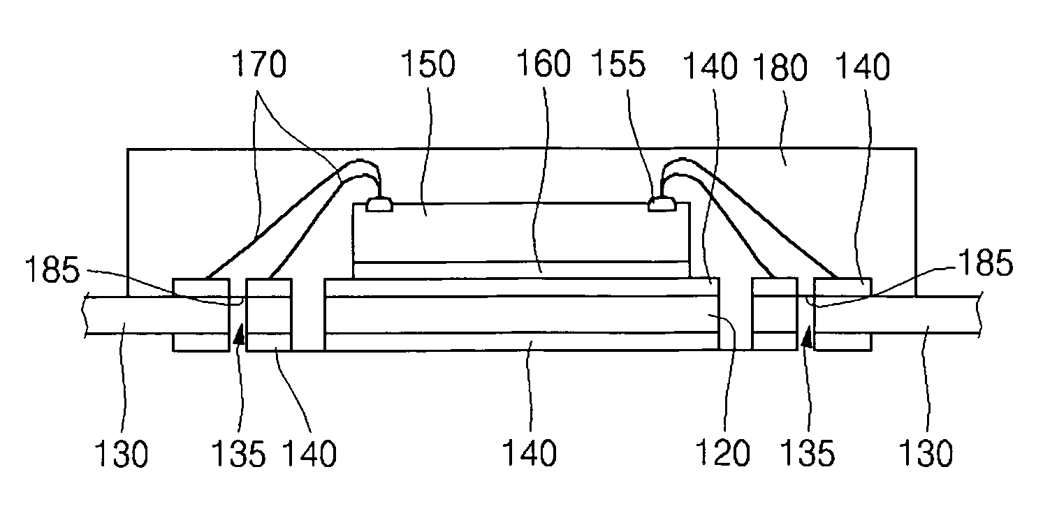
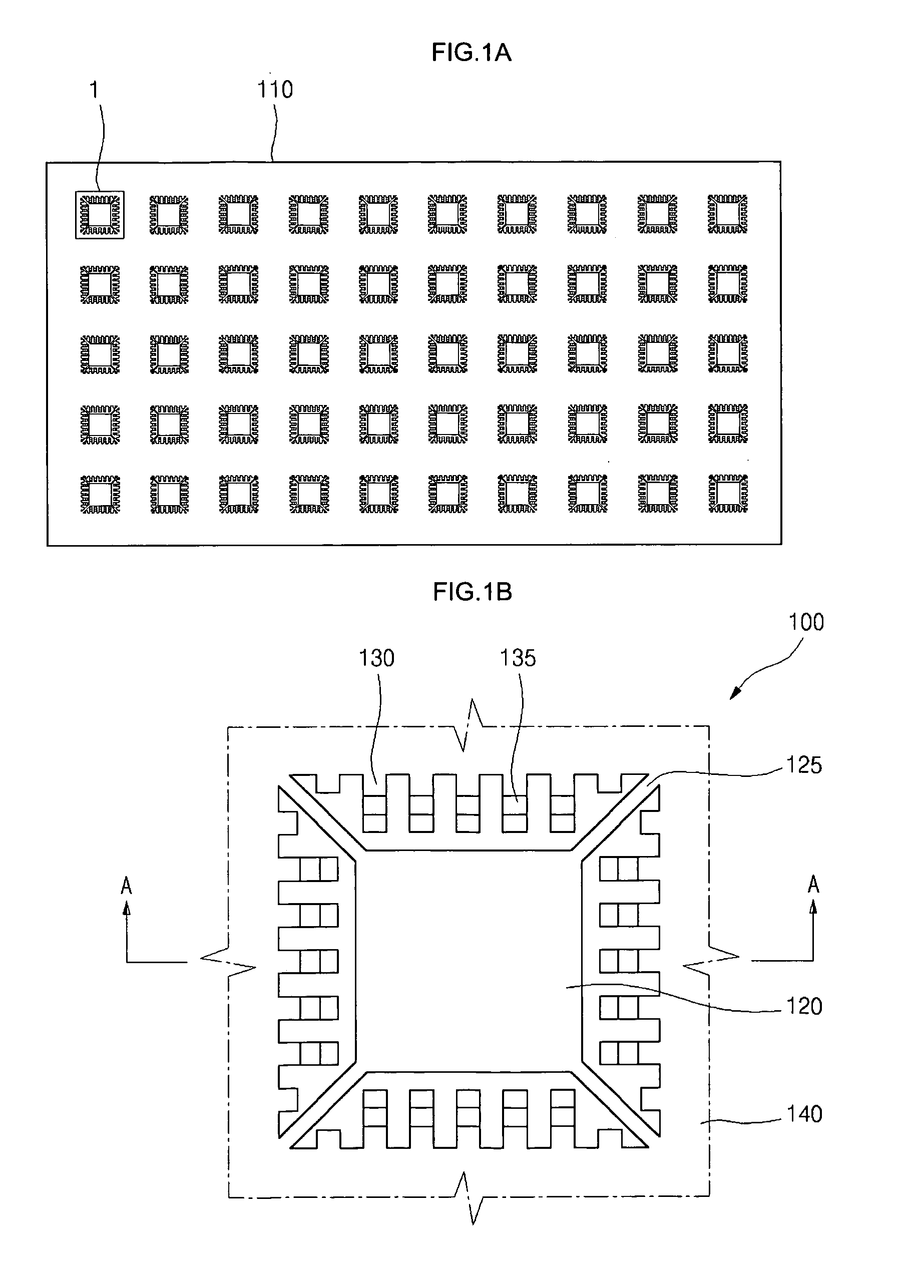
[0033]Referring now to the drawings wherein the showings are for purposes of illustrating preferred embodiments of the present invention only, and not for purposes of limiting the same, FIG. 1A is a top plan view of a leadframe strip having multiple leadframes 100 thereon which are each formed in accordance with the present invention. The leadframe strip comprises a plate 110 which is preferably fabricated from copper, copper alloy, or an equivalent thereof, though the present invention is not intended to be limited to any particular material for the plate 110. The copper plate 110 is subjected to a chemical etching or mechanical stamping process as facilitates the formation of the individual leadframes 100 thereon. As seen in FIG. 1A, the leadframes 100 are arranged in a matrix-like pattern defining multiple vertical columns and horizontal rows. Those of ordinary skill in the art will recognize that the 5×10 matrix including a total of 50 leadframes 100 formed in the copper plate 1...
second embodiment
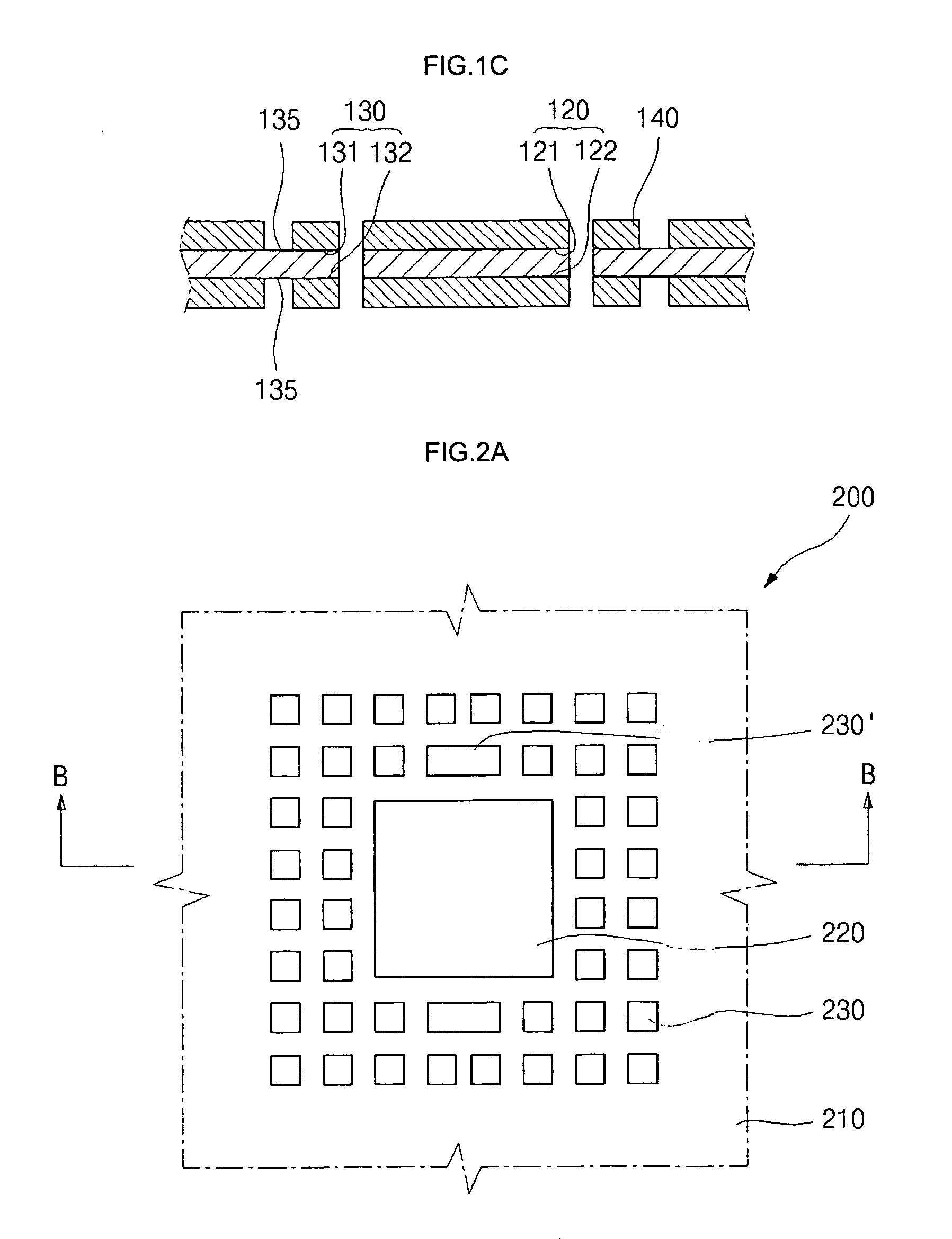
[0047]Referring now to FIGS. 2A and 2B, there is shown a leadframe 200 which is formed in accordance with the present invention. The leadframe 200 comprises a copper plate 210 which has a generally planar first (top) surface 211 and an opposed, generally second (bottom) surface 212. In addition to the copper plate 210, the leadframe 200 comprises a die paddle 220 which preferably has a generally quadrangular shape defining four sides or peripheral edge segments. Though the die paddle 220 is shown in FIG. 2A as having a generally square configuration, those of ordinary skill in the art will recognize that the die paddle 220 may alternatively have any rectangular, octagonal, or circular shape, the present invention not being limited to any particular shape for the die paddle 220.
[0048]The leadframe 200 further comprises a plurality of leads 230. As seen in FIGS. 2A and 2B, the leads 230 are arranged in an inner set which circumvents the die paddle 220, and an outer set which circumven...
third embodiment
[0059]Referring now to FIGS. 3A and 3B, there is shown a leadframe 300 which is formed in accordance with the present invention. The leadframe 300 comprises a copper plate 310 which has a generally planar first (top) surface 311 and an opposed, generally second (bottom) surface 312. In addition to the copper plate 310, the leadframe 300 comprises a die paddle 220 which preferably has a generally quadrangular shape defining four sides or peripheral edge segments. Though the die paddle 320 is shown in FIG. 3A as having a generally square configuration, those of ordinary skill in the art will recognize that the die paddle 320 may alternatively have any rectangular, octagonal, or circular shape, the present invention not being limited to any particular shape for the die paddle 320.
[0060]The leadframe 300 further comprises a plurality of leads 330. As seen in FIGS. 3A and 3B, the leads 330 are arranged in an inner set which circumvents the die paddle 320, and an outer set which circumven...
PUM
| Property | Measurement | Unit |
|---|---|---|
| conductive | aaaaa | aaaaa |
| electrically | aaaaa | aaaaa |
| area | aaaaa | aaaaa |
Abstract
Description
Claims
Application Information