Semiconductor device and method of manufacturing the same

a semiconductor and semiconductor technology, applied in the field of semiconductor devices, can solve the problems of crystal defect, lowering of breakdown voltage, deterioration of transistor characteristics in the application of high current, etc., and achieve the effect of high breakdown voltage performance of transistors

Inactive Publication Date: 2007-05-08
HITACHI LTD
View PDF5 Cites 4 Cited by
  • Summary
  • Abstract
  • Description
  • Claims
  • Application Information

AI Technical Summary

Benefits of technology

[0013]According to the present invention it is possible to provide a heterobipolar transistor capable of suppressing an abrupt lowering of current gain and cut-off frequency in the application of a high current while maintaining a high breakdown voltage performance of the transistor.

Problems solved by technology

As described above, in what is called a double heterobipolar transistor having two heterointerfaces, the deterioration of transistor characteristics in the application of a high current has been an unavoidable problem.
However, an increase of collector concentration causes a lowering of breakdown voltage and an increase in thickness of the silicon-germanium layer is likely to cause crystal defect due to accumulation of strain.
Thus, any of those methods cannot be the best solution.

Method used


Image

  • Semiconductor device and method of manufacturing the same
  • Semiconductor device and method of manufacturing the same
  • Semiconductor device and method of manufacturing the same

Examples


Embodiment Construction

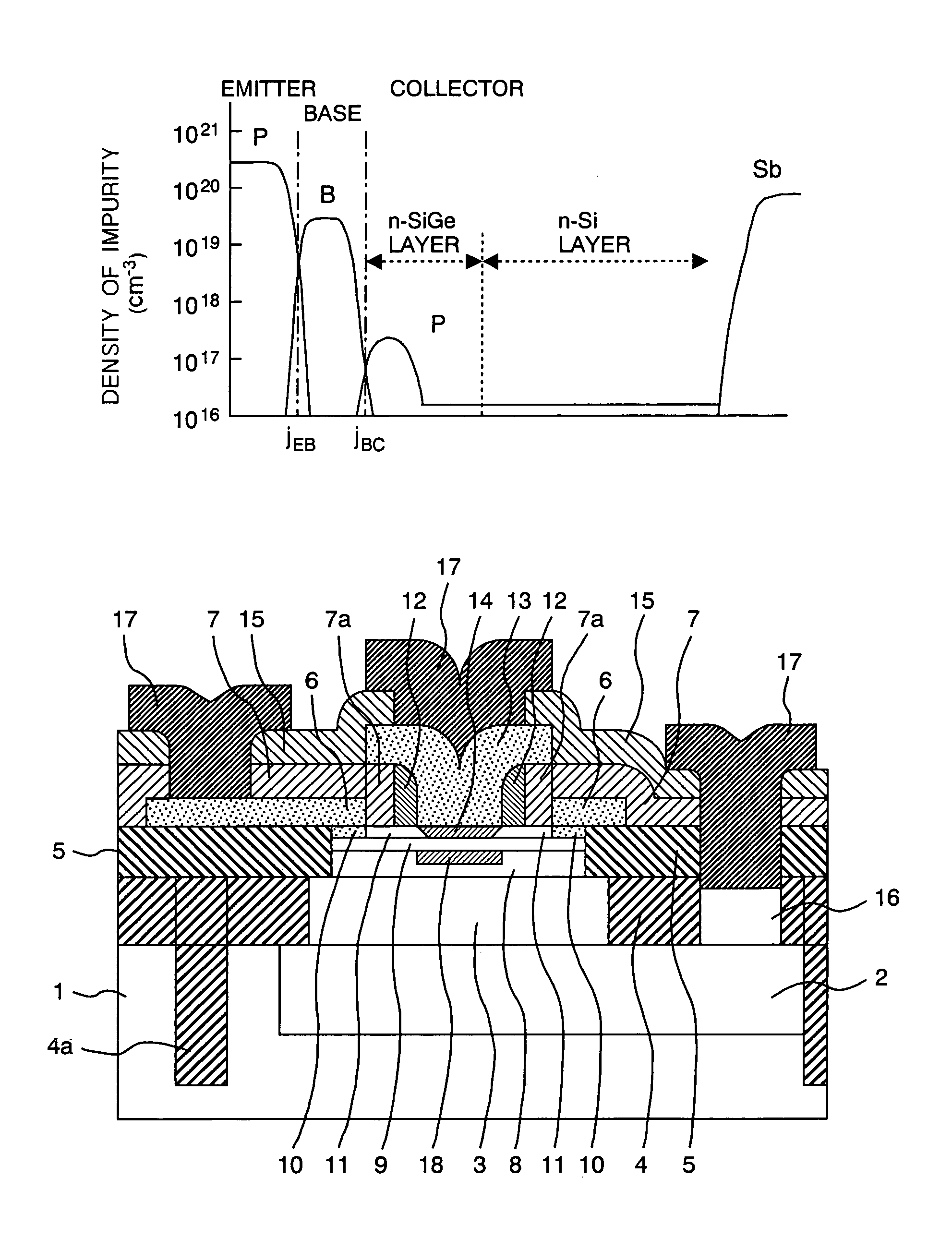
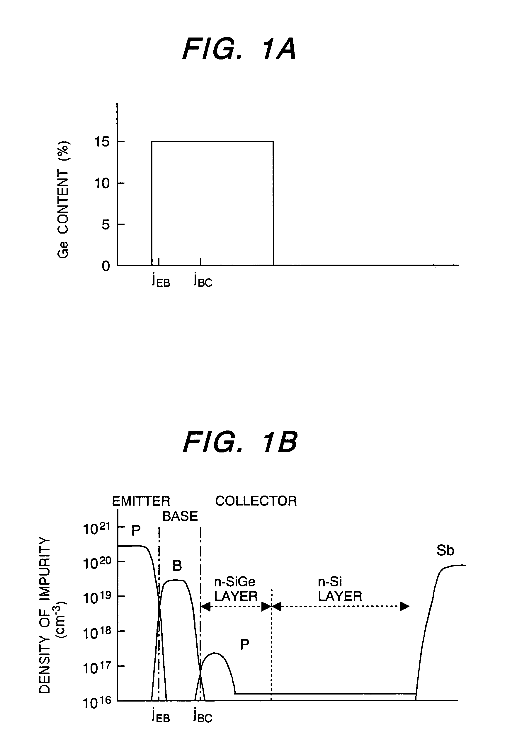
[0031]Preferred embodiments of the present invention are characterized in that, in a heterobipolar transistor having a silicon-germanium layer, the collector impurity concentration has a peak within an n-type silicon-germanium layer and that the value of the peak is higher than the collector impurity concentration in an n-type silicon layer. Further, during operation of the transistor, a collector-base depletion layer on the collector side extends up to the n-type silicon layer and the transistor has a high breakdown voltage. In the present invention, the occurrence of a barrier in a conduction band can be delayed by providing a high concentration impurity region in a collector layer located on the base side rather than heterojunction, and a satisfactory transistor operation can be ensured in a higher current. Further, a lowering in breakdown voltage of the transistor is prevented by limiting a high concentration collector region.

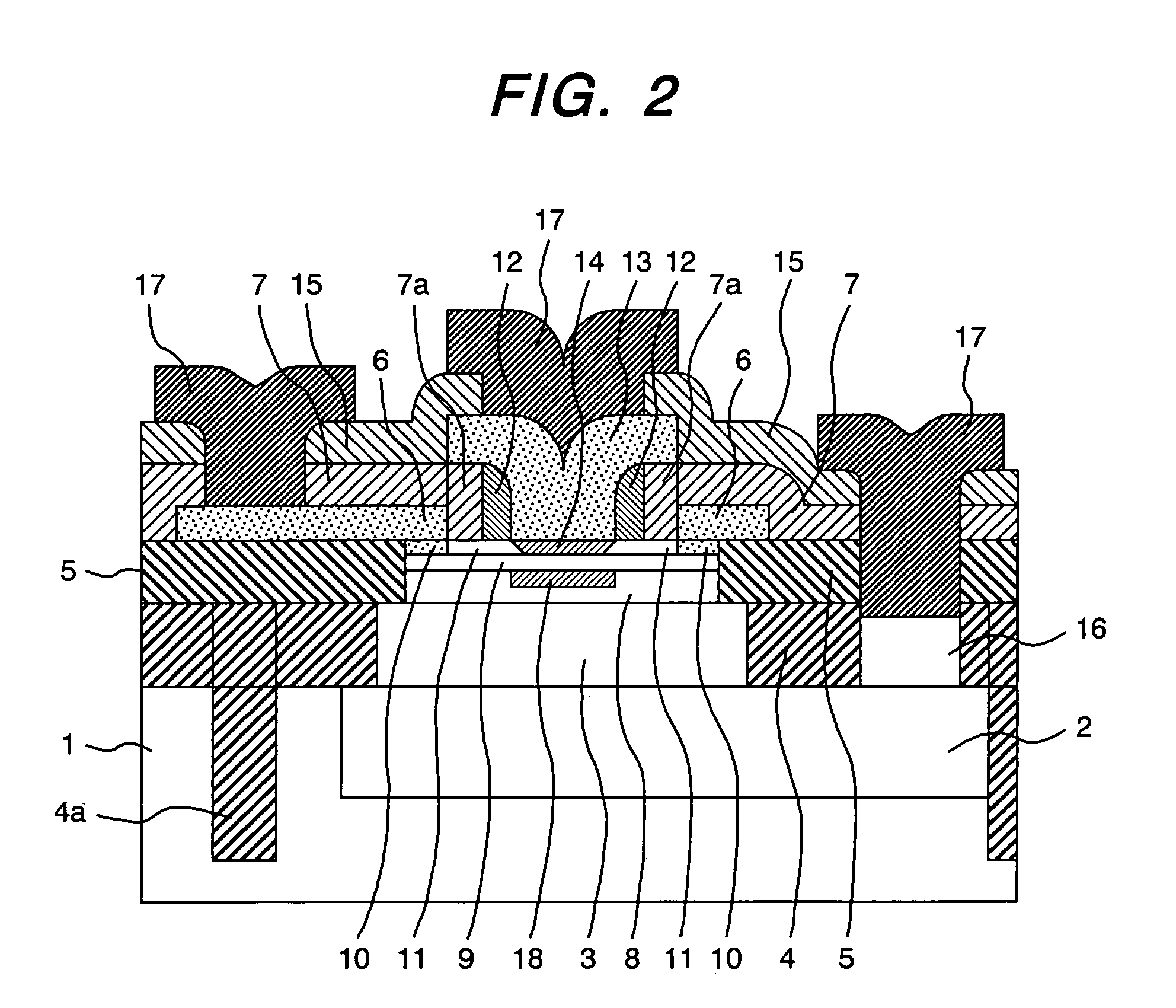
[0032]Concrete embodiments of the semiconductor devic...


PUM


Abstract

A bipolar type semiconductor device capable of attaining high current gain and high cut-off frequency and performing a satisfactory transistor operation also in a high current region while maintaining a high breakdown voltage performance, as well as a method of manufacturing the semiconductor device, are provided. In a collector comprising a first semiconductor layer and a second semiconductor layer narrower in band gap than the first semiconductor layer, an impurity is doped so as to have a peak of impurity concentration within the second collector layer and so that the value of the peak is higher than the impurity concentration at any position within the first collector layer. It is preferable to adjust the concentration of the doped impurity in such a manner that a collector-base depletion layer extends up to the first collector layer.

Description

CLAIM OF PRIORITY[0001]The present application claims priority from Japanese application JP 2004-251535 filed on Aug. 31, 2004, the content of which is hereby incorporated by reference into this application.BACKGROUND OF THE INVENTION[0002]1. Field of the Invention[0003]The present invention relates to a semiconductor device, especially a bipolar transistor, and a method of manufacturing the same.[0004]2. Description of the Prior Art[0005]Recently, bipolar transistors and integrated circuits with bipolar transistors mounted thereon have been utilized in various application fields. The bipolar transistor is advantageous over the field effect transistor in terms of high speed performance and high breakdown voltage performance, and its application is expanded for communication devices, storage systems, etc. Conventional examples of a bipolar transistor capable of attaining high speed and high breakdown voltage include a silicon-germanium heterobipolar transistor using the selective epi...

Claims


Application Information

Patent Timeline
Patent Type & Authority Patents(United States)
IPC IPC(8): H01L31/0328H01L31/0336H01L31/072H01L31/109H01L21/331H01L29/732H01L29/737
CPCH01L29/0821H01L29/66242H01L29/7378
Inventor MIURA, MAKOTOWASHIO, KATSUYOSHISHIMAMOTO, HIROMI
Owner HITACHI LTD
Why Eureka
Try Eureka