Circuit and method for suppression of electromagnetic coupling and switching noise in multilayer printed circuit boards

a multi-layer printed circuit board and electromagnetic coupling technology, applied in the incorporation of printed capacitors, line-transmission details, waveguide devices, etc., can solve the problems of increasing material and manufacturing costs with increasing concomitantly, and achieve the effect of eliminating power plane resonance and suppressing digital nois

Inactive Publication Date: 2007-05-08
WEMTEC
View PDF50 Cites 123 Cited by
  • Summary
  • Abstract
  • Description
  • Claims
  • Application Information

AI Technical Summary

Benefits of technology

[0012]By way of introduction only, the present embodiments provide a two-dimensional, periodic, metallic structure, which acts as a distributed microwave bandstop filter integrated into a parallel-plate waveguide. These embodiments can be used as an electromagnetic interference (EMI) filter to suppress digital noise on power planes, as well as to eliminate power plane resonances. Hence, they may be used for EMI and EMC (electromagnetic compatibility) purposes in printed circuit boards.
[0013]In particular embodiments, the new structure may be formed as part of a printed circuit board (PCB) power distribution network to reduce noise coupled from digital switching circuits to power and ground planes of the PCB. A lower conductive plate is used as one plane and an upper conductive plate is used as the other plane. An array of conductive patches and an array of conductive vias or rods are positioned between the plates and intervening dielectric layers. By tailoring the permittivity and thickness of the dielectric layers within the structure, as well as the patch size and via diameter, and the size, number, and / or distribution of the conductive vias these structures may be optimized to produce a stopband in which TEM mode propagation is suppressed over desired frequency ranges. Furthermore, these TEM mode suppression circuits can be made thinner than known suppression circuits by more than one order of magnitude for the same or better electrical performance.
[0015]The new structure, when used as part of a printed circuit board design, permits elimination of many of the higher frequency surface-mounted bypass capacitors used in conventional PCB designs, along with the concomitant increased material and manufacturing costs. Also, the new structure offers significantly improved RF isolation over frequency bands unattainable in conventional designs using bypass capacitors alone.

Problems solved by technology

The new structure, when used as part of a printed circuit board design, permits elimination of many of the higher frequency surface-mounted bypass capacitors used in conventional PCB designs, along with the concomitant increased material and manufacturing costs.

Method used


Image

  • Circuit and method for suppression of electromagnetic coupling and switching noise in multilayer printed circuit boards
  • Circuit and method for suppression of electromagnetic coupling and switching noise in multilayer printed circuit boards
  • Circuit and method for suppression of electromagnetic coupling and switching noise in multilayer printed circuit boards

Examples


first embodiment

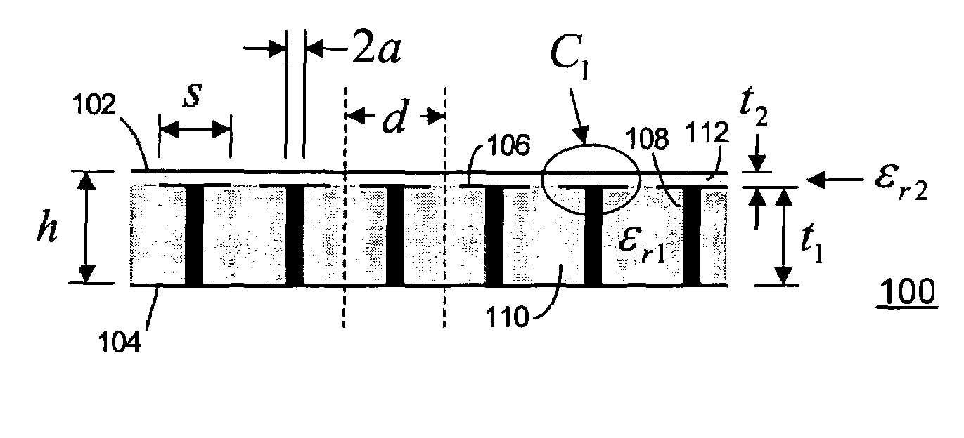
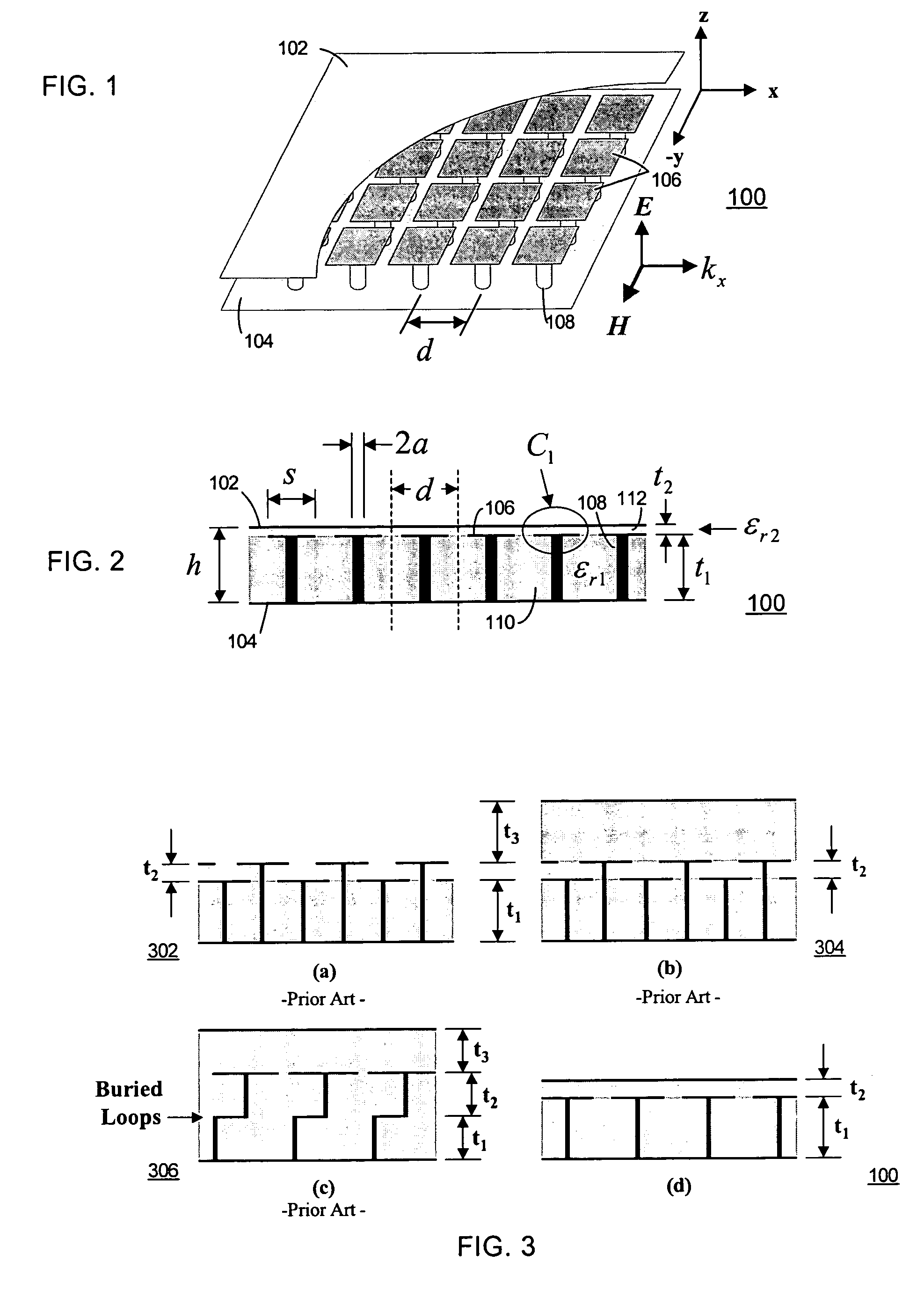
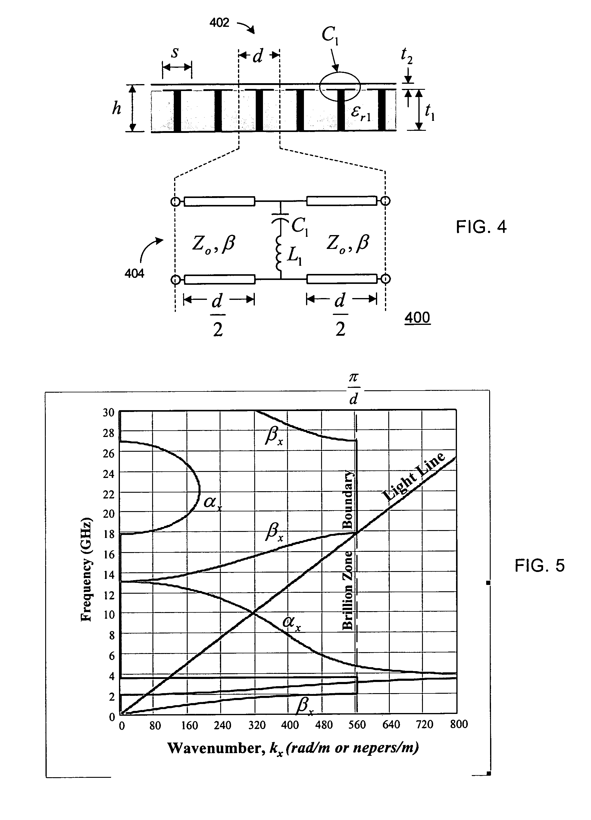
[0051]Referring now to the drawing, FIG. 1 and FIG. 2 illustrate a parallel plate wave guide (PPW) 100 containing a transverse electromagnetic (TEM) mode suppression circuit. FIG. 1 is a perspective view of the PPW 100 and FIG. 2 is a cross-sectional view of the PPW 100. Coordinate axes establish the x, y and z directions as used herein.

[0052]As shown in FIGS. 1 and 2, the PPW 100 includes an upper conductive plate 102, a lower conductive plate 104, an array of conductive coplanar patches 106 located a distance t2 from the upper plate 102, an array of conductive rods or vias 108 of length t1 and radius a that connect the lower plate 104 to the center of each patch 106, a first dielectric layer 110 and a second dielectric layer 112. The patches 106 are illustrated to be squares of side length s in FIG. 1, but other shapes such as rectangular, hexagonal, triangular, circular, etc. can be used. The patch realizes a parallel-plate capacitance between the end of the rod 108 below it and ...

fourth embodiment

[0123]Yet another embodiment involves adding a spiral inductor in series with each via, as shown in FIGS. 16 and 17. The purpose of this added inductance is to reduce flower. FIG. 16 and FIG. 17 illustrate a parallel plate waveguide (PPW) 1600. The PPW 1600 includes an upper conductive plate and a lower conductive plate (not shown in FIG. 16). The PPW 1600 includes an array of conductive coplanar patches 1606 located a distance t2 from the upper plate, an array of conductive rods or vias 1608 of length t1 and radius a that connect the lower plate to the center of each patch 1606, a first dielectric layer 1610 and a second dielectric layer 1612. The PPW 1600 further includes a spiral inductor 1612 associated with each respective patch 1606 and via 1608.

[0124]In the embodiment of FIGS. 16 and 17, the inductors 1614 and patches are coplanar and are etched as part of the same metal layer. The coplanar spiral inductor 1614 is formed within the perimeter of the patch 1606. The merit of an...


PUM


Abstract

Apparatus for suppressing noise and electromagnetic coupling in the printed circuit board of an electronic device includes an upper conductive plate and an array of conductive coplanar patches positioned a distance t2 from the upper conductive plate. The distance t2 is chosen to optimize capacitance between the conductive coplanar patches and the upper conductive plate for suppression of noise or electromagnetic coupling. The apparatus further includes a lower conductive plate a distance t1 from the array of conductive coplanar patches and conductive rods extending from respective patches to the lower conductive plate.

Description

REFERENCE TO RELATED APPLICATIONS[0001]The present patent application claims the benefit of the filing date under 35 U.S.C. § 119(e) of Provisional U.S. Patent Application Ser. No. 60 / 477,152 filed Jun. 9, 2003, entitled “Circuit and Method For Suppression of Transverse Electromagnetic Modes” and is related to U.S. patent application Ser. No. 10 / 167,954 filed Jun. 12, 2002, entitled “Aperture Antenna Having a High-Impedance Backing” which claims the benefit of the filing date under 35 U.S.C. § 119(e) of Provisional U.S. Patent Application Ser. No. 60 / 298,654, filed on Jun. 15, 2001. All of the foregoing applications are hereby incorporated herein in their entirety by this reference.BACKGROUND[0002]This invention is related generally to reduction of noise induced in power planes due to switching of digital circuits. More particularly, the present invention is related to circuits and method for suppression of transverse electromagnetic modes in parallel plate waveguides.[0003]A common...

Claims


Application Information

Patent Timeline
Patent Type & Authority Patents(United States)
IPC IPC(8): H01L29/40H01L23/58H01L23/62H01P1/16H04B3/04H05KH05K1/16
CPCH01P1/16H01P1/2005H05K1/162H05K2201/093H05K2201/09309H05K2201/09663
Inventor MCKINZIE, III, WILLIAM E.ROGERS, SHAWN D.
Owner WEMTEC
Why Eureka
Try Eureka