Stacked die BGA or LGA component assembly

a technology of stacked dies and components, applied in the direction of electrical equipment, semiconductor devices, semiconductor/solid-state device details, etc., can solve the problems of high pin count on circuit boards, large area occupied by interconnected dies, and many wires that are required

Inactive Publication Date: 2007-05-08
INVENSAS CORP
View PDF102 Cites 95 Cited by
  • Summary
  • Abstract
  • Description
  • Claims
  • Application Information

AI Technical Summary

Problems solved by technology

However, in order to create the necessary interconnections between the die, many wires are required that are extremely thin and difficult to create.
Furthermore, the resulting interconnected die occupy a very large area, or footprint, on the electronic systems circuit board onto which the wafer scale integration device is attached for connection into the electronic system.
This method results in an unusually high pin count on the circuit board which reduces the reliability of the circuitry because the high pin count increases the possibility that one of the many pins may become disconnected from the board.
This method of rerouting leads offers improvement in circuit density over prior methods but is complex and expensive.
In addition, the rerouting leads extend over adjacent die, which are destroyed when the modified chip is cut out of the wafer.
The use of solid feed-throughs to interconnect wafers may cause damage to the array due to differential thermal coefficients of expansion during thermal cycles.
Furthermore, the process is costly and makes the wafers difficult to separate for repairs.
Furthermore, for some applications, it may not be desirable to use stacks of entire wafers due to size constraints of the electrical device.
There are a number of methods for stacking packaged integrated circuits, but in general, they suffer from a size disadvantage, and a performance disadvantage, due to the added electrical parasitics arising from the necessary lengths and characteristics of the inter-package interconnections.
Stacks of packaged integrated circuits have been recently popular but take up too much board space, are too thick, and will not operate at the high speeds being required by advanced memory devices such as DDR2 and DDR3 DRAM.

Method used


Image

  • Stacked die BGA or LGA component assembly
  • Stacked die BGA or LGA component assembly
  • Stacked die BGA or LGA component assembly

Examples


Embodiment Construction

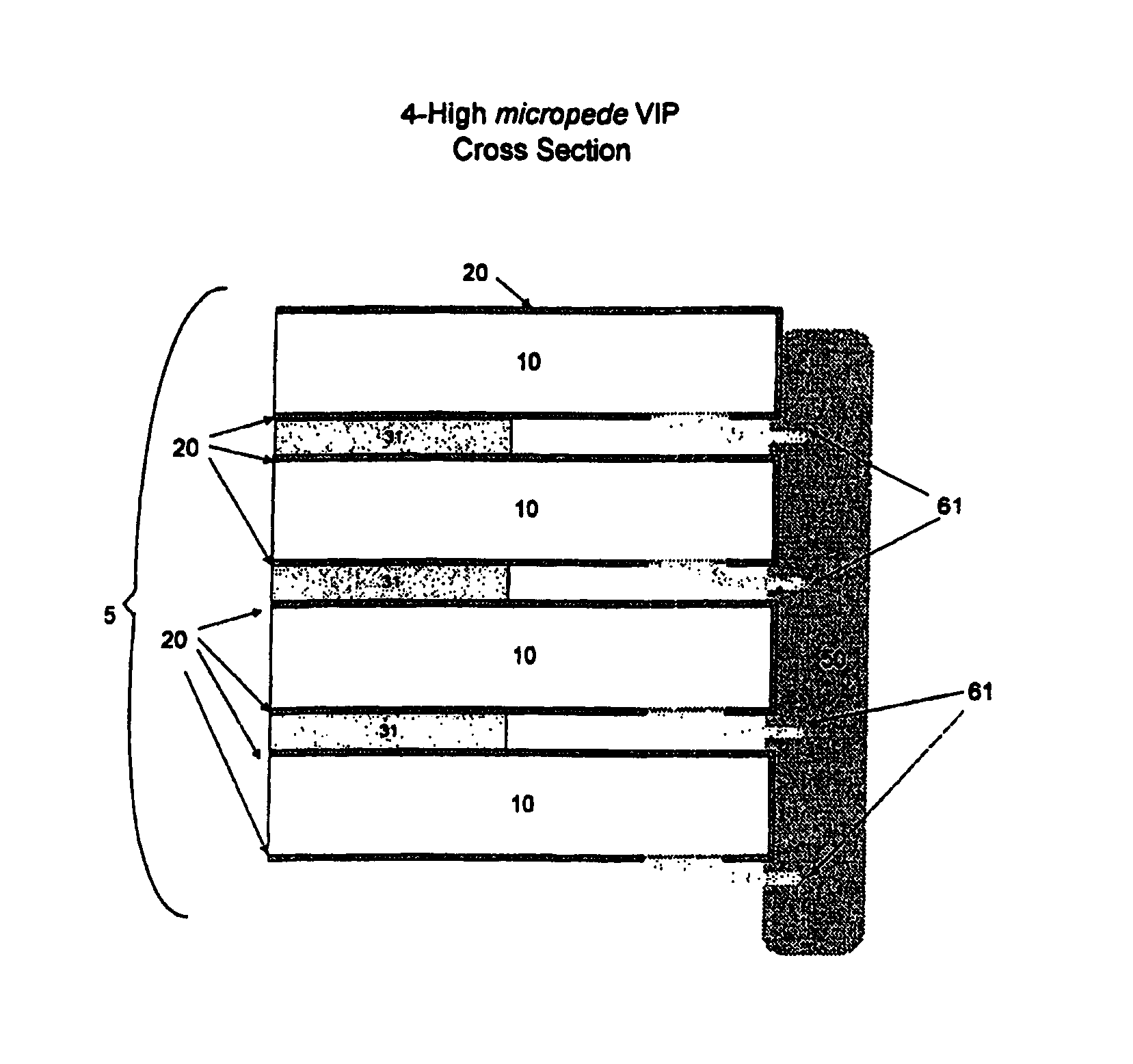
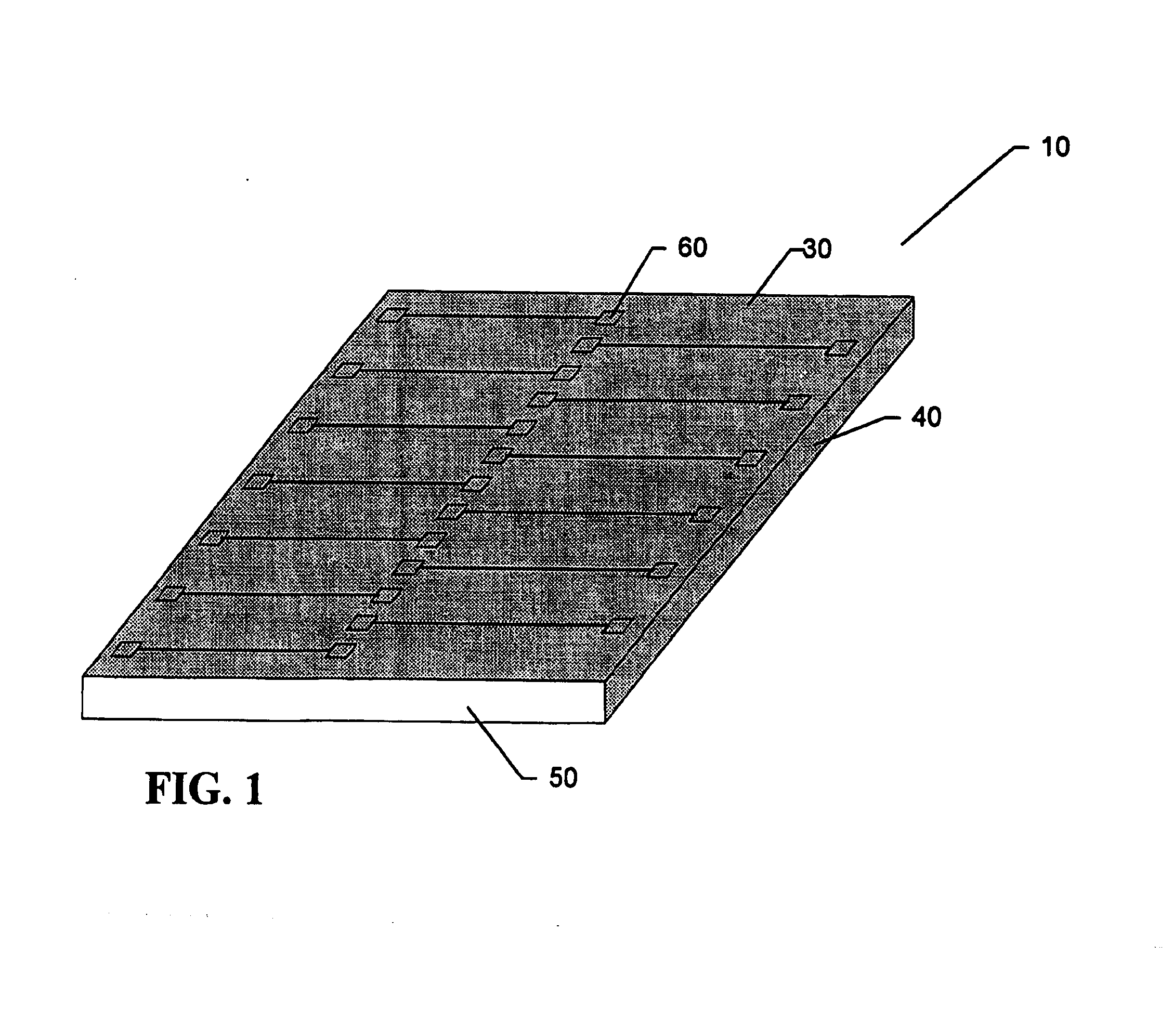
[0022]Referring to FIG. 1, semiconductor die 10, with original connection pads 60 have had an insulating layer applied to the top surface, 30 of all of the die while the die are still connected together in a wafer form. A metal layer is deposited and defined using photolithography, to reroute the electrical signals from the original connection pads 60 to new locations at the edge of the die. An additional layer of insulating material is optionally applied above the metal layer, and openings are made in the top layer of insulating material at the relocated pad locations at the edge of the semiconductor die, and optionally at the original pad locations down the center of the top surface of the die.

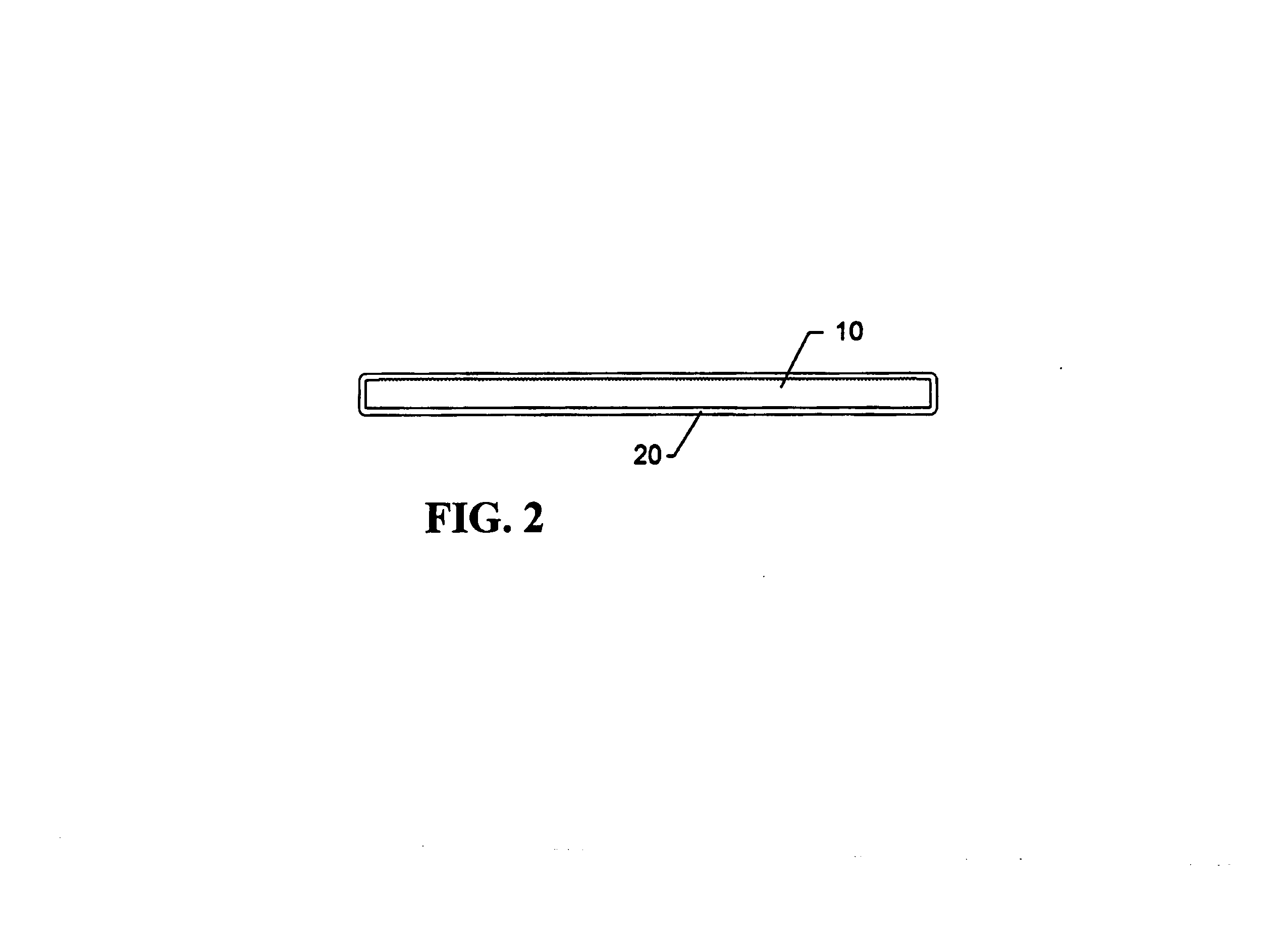
[0023]Referring to FIG. 2, the semiconductor die, 10, has been thinned by grinding or lapping, and has been singulated from the semiconductor wafer, and said semiconductor die has been coated with a conformal insulating coating 20.

[0024]Referring to FIG. 3, openings have been made in the coa...


PUM


Abstract

The present invention provides an apparatus for vertically interconnecting semiconductor die, integrated circuit die, or multiple die segments. Metal rerouting interconnects which extend to one or more sides of the die or segment can be optionally added to the die or multi die segment to provide edge bonding pads upon the surface of the die for external electrical connection points. After the metal rerouting interconnect has been added to the die on the wafer, the wafer is optionally thinned and each die or multiple die segment is singulated from the wafer by cutting or other appropriate singulation method. After the die or multiple die segments are singulated or cut from the wafer, insulation is applied to all surfaces of the die or multiple die segments, openings are made in the insulation above the desired electrical connection pads, and the die or multiple die segments are placed on top of one another to form a stack. Vertically adjacent segments in the stack are electrically interconnected by attaching a short flexible bond wire or bond ribbon to the exposed electrical connection pad at the peripheral edges of the die which protrudes horizontally from the die and applying electrically conductive polymer, or epoxy, filaments or lines to one or more sides of the stack.

Description

CROSS REFERENCE TO RELATED APPLICATIONS [0001]The present application is related to provisional patent application No. 60 / 561,849, filed Apr. 13, 2004 entitled “Stacked Die BGA or LGA Component Assembly”, the details of which are hereby incorporated by reference, and the benefit of the earlier Apr. 13, 2004 filing date is claimed in accordance with 35 USC 119 (e) (1).BACKGROUND OF THE INVENTION [0002]The present invention relates to an apparatus for stacking and interconnecting integrated circuit die and / or multiple die segments of silicon, interconnecting the die and or multiple die segments on the edges of the stack using an electrically conductive polymer or epoxy, and mounting the stack of die on a BGA substrate.[0003]For many years, electrical components such as transistors and integrated circuits have been made using wafers of semiconductor material, including silicon and / or germanium. Integrated circuits have been provided on the wafer using various techniques known as etchin...

Claims


Application Information

Patent Timeline
Patent Type & Authority Patents(United States)
IPC IPC(8): H01L23/02H01L21/56H01L23/31H01L23/525H01L25/065
CPCH01L21/563H01L25/00H01L23/525H01L25/0657H01L23/34H01L23/3128H01L2224/24145H01L2224/73203H01L2225/06513H01L2225/06517H01L2225/06524H01L2225/06551H01L2225/06582H01L2225/06586H01L2924/01046H01L2924/01079H01L2924/09701H01L2924/15311H01L2924/3011H01L23/02H01L23/28
Inventor VINDASIUS, ALROBINSON, MARCJACOBSEN, LARRYALMEN, DONALD
Owner INVENSAS CORP
Why Eureka
Try Eureka