Liquid crystal on silicon display with micro color filters positioned on the top surface of the transparent substrate

a liquid crystal display and transparent substrate technology, applied in non-linear optics, instruments, optics, etc., can solve the problems of inability to easily remove heat generated by the color filter, and achieve the effect of reducing the fabricating cost of the display panel, and avoiding the heat generation of the color filter

Active Publication Date: 2007-05-08
UNITED MICROELECTRONICS CORP
View PDF9 Cites 49 Cited by
  • Summary
  • Abstract
  • Description
  • Claims
  • Application Information

AI Technical Summary

Benefits of technology

[0008]It is therefore a primary objective of the claimed invention to provide an LCOS display panel that has a better performance of heat irradiating and lower cost to solve the above-mentioned problem.
[0010]It is an advantage of the claimed invention that the micro color filters are positioned on the top surface of the transparent substrate, so that heat does not accumulate in the inner portion of the display panel to overheat the display panel that causes damage to the inner elements. Furthermore, the heat generated by the micro color filters positioned on the display panel can be easily removed by an outer cooling system, such as a cooling fan, to maintain a preferable temperature of the display panel. On the other hand, when the micro color filters are positioned on the top surface of the transparent substrate, an AR coating can be substituted so as to decrease the fabricating cost of the display panel.

Problems solved by technology

However, no matter if the color filter 20 is positioned between the glass substrate 14 and the transparent conductive layer 18, or between the transparent conductive layer 18 and the alignment in the prior art, it causes a disadvantage of heat generated by the color filter 20 when the LCOS panel 10 is operating accumulating in the inner portion of the LCOS panel 10 because the heat cannot be removed by an outer cooling system easily.
Therefore, how to design a structure of the LCOS panel for improving the performance of heat radiation so as to extend the longevity of the elements of the LCOS panel is still an important issue for manufacturers.

Method used


Image

  • Liquid crystal on silicon display with micro color filters positioned on the top surface of the transparent substrate
  • Liquid crystal on silicon display with micro color filters positioned on the top surface of the transparent substrate
  • Liquid crystal on silicon display with micro color filters positioned on the top surface of the transparent substrate

Examples


Embodiment Construction

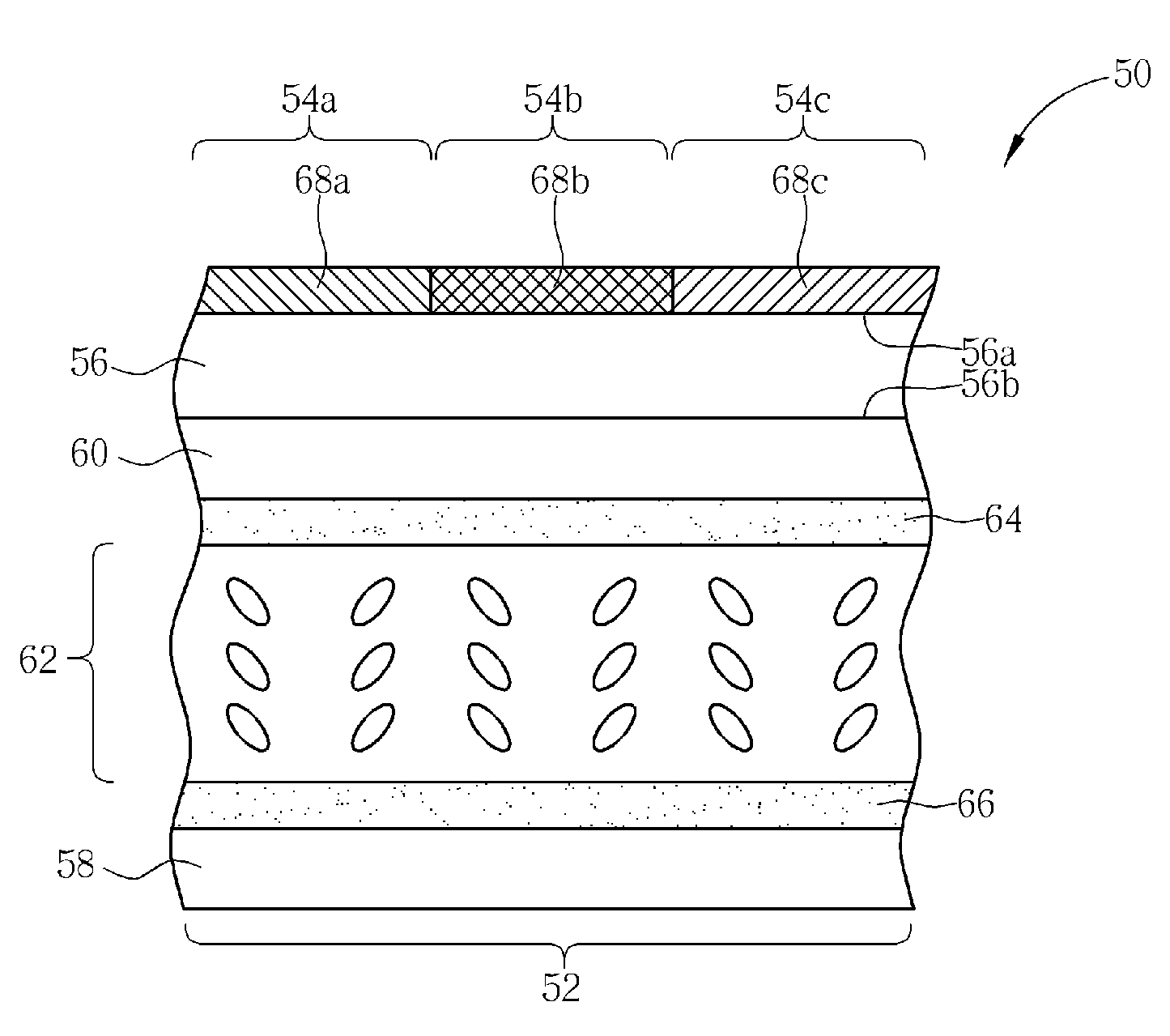
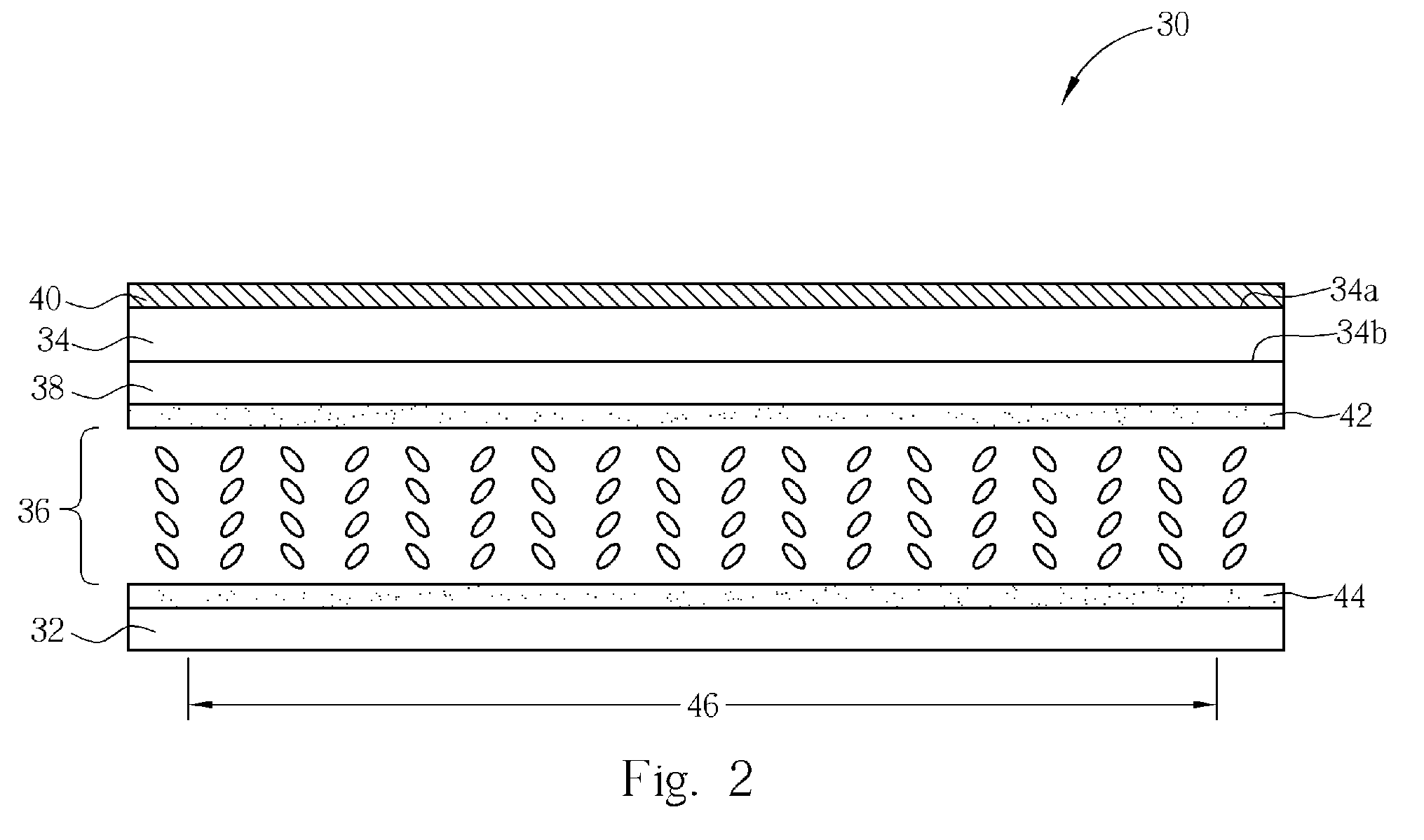
[0015]Please refer to FIG. 2. FIG. 2 is a section view of an LCOS panel 30 according to the present invention. LCOS panel 30 comprises a silicon substrate 32, a transparent substrate 34 positioned above the silicon substrate 32, and a liquid crystal layer 36 positioned between the silicon substrate 32 and the transparent substrate 34. The silicon substrate 32 has a pixel region 46 thereon and a plurality of MOS transistors and corresponding pixels (not shown) are positioned in the pixel region 46. The transparent substrate 34 has a top surface 34a and bottom surface 34b. On the bottom surface 34b of the transparent substrate 34 is a transparent conductive layer 38, such as an indium tin oxide (ITO) layer. A top alignment layer 42 and a bottom alignment layer 44 are positioned between the liquid crystal layer 36 and the transparent conductive layer 38, and between the liquid crystal layer 36 and the silicon substrate 32 respectively for adjusting the arrangement directions of the liq...


PUM

PropertyMeasurementUnit
transparentaaaaaaaaaa
photosensitiveaaaaaaaaaa
specific spectrumaaaaaaaaaa

Abstract

An LCOS display panel includes a silicon substrate having a plurality of pixels arranged in a pixel array thereon, a transparent substrate positioned above the silicon substrate, a liquid crystal layer positioned between the transparent substrate and the silicon substrate, and a plurality of micro color filters positioned on the top surface of the transparent substrate and corresponding to subpixels of the pixels.

Description

BACKGROUND OF INVENTION[0001]1. Field of the Invention[0002]The invention relates to a liquid crystal on silicon display (LCOS display), and more particularly, to an LCOS display having color filters positioned on the top surface of the cover substrate.[0003]2. Description of the Prior Art[0004]LCOS display technology is the key of reflective LCOS projectors and rear-projection televisions. The advantages of LCOS micro-displays are a tiny size, high resolution, low power, low cost, etc. The difference between an LCOS display and a conventional thin film transistor-liquid crystal display (TFT-LCD) is materials used for forming substrates. Both a cover substrate and a backplane are made of glass in a TFT-LCD. Nevertheless, the cover substrate in an LCOS display is made of glass, but the backplane in an LCOS display is a semiconductor silicon substrate. Therefore, an LCOS process combines LCD techniques and complementary metal-oxide semiconductor (CMOS) processes.[0005]The main structu...

Claims


Application Information

Patent Timeline
Patent Type & Authority Patents(United States)
IPC IPC(8): G02F1/1335
CPCG02F1/133514G02F1/136277G02F1/133385G02F2001/133562G02F1/133562
Inventor KUAN, TA-SHUANGCHAN, CHIA-TSUNGLIN, CHIA-TE
Owner UNITED MICROELECTRONICS CORP
Why Eureka
Try Eureka