Integrated driving, receiving, controlling, and monitoring for optical transceivers

a technology of optical transceivers and integrated drives, which is applied in the direction of electromagnetic transmission, electromagnetic transceivers, electrical apparatus, etc., can solve the problems of increasing increasing the cost of optical transceivers and the requirement for pcb area, and reducing the size of optical transceivers

Active Publication Date: 2007-05-08
NASA +1
View PDF95 Cites 161 Cited by
  • Summary
  • Abstract
  • Description
  • Claims
  • Application Information

AI Technical Summary

Benefits of technology

[0012]In one embodiment, the laser driver is a variable laser driver having a wide driving flexibility and can be set to drive one of a plurality of semiconductor lasers. The variable laser driver can be set to drive one of a vertical cavity surface emitting laser (VCSEL), a Fabry-Perot (FP) laser, and a distributed feedback (DFB) laser. In another embodiment, the laser driver has a selectable output mode including a first output mode and a second output mode, the output mode being selected in response to the selection of laser diode and the connection between packaging pins of the single integrated circuit chip and pins of the laser diode. The first output mode of the laser driver is to drive vertical cavity surface emitting lasers, and the second output mode of the laser driver is to drive Fabry-Perot (FP) lasers and distributed feedback (DFB} lasers. The laser driver can operate over a wide range of data rates from 100 Mbps through 4.5 Gbps. Similarly, the limiting amplifier can operate over a wide range of data rates from 100 Mbps through 4.5 Gbps in one embodiment. In another embodiment, the limiting amplifier operates over data rates from 1 Gbps through 4.5 Gbps. The limiting amplifier includes a rate selection pin to switch in a bandwidth limiting filter in order to operate at a data rate of less than 2.5 Gbps or 1.3 Gbps. In another embodiment, an electric subassembly (ESA) is included as part of an optical transceiver. The electric subassembly (ESA) includes an optical transceiver integrated circuit and a non-volatile memory integrated circuit. The optical transceiver integrated circuit is a single device that integrates a laser driver, a limiting amplifier, and a micro-controller coupled together in a single semiconductor substrate. The optical transceiver integrated circuit couples to a transmit optical subassembly (TOSA) and a receive optical subassembly (ROSA) of the optical transceiver in order to transceive data signals over an optical data link. The non-volatile memory integrated circuit is coupled to the optical transceiver integrated circuit in order to store information related to the operation of the optical transceiver in a non-volatile manner so that it is not lost when power is shut off or lost to the optical transceiver. The non-volatile memory integrated circuit may additionally be used to store micro-controller program coding and transceiver operational parameters.
[0016]The integrated circuit may further include a digital data input / output port to transfer the one or more laser diode operational parameters stored in the memory to a host system and to transfer the one or more current laser diode parameters from the one or more A / D converters to the host system so the host system can perform an advanced replacement algorithm to determine when to replace the optical transceiver in advance of a failure. The digital data input / output port may further allow the host to access the non-volatile memory to store a unique identifier identifying the optical transceiver. The digital data input / output port may further allow the host to access the non-volatile memory to read any advanced replacement flag, failed flag, and any reason indicator.
[0018]In another embodiment, a method for an optical transceiver is disclosed. The method includes monitoring a sequence of laser diode parameters for a laser diode within the optical transceiver; determining a change in the sequence of laser diode parameters to provide an advanced warning of failure; and generating an advance replacement indicator for the optical transceiver in response to determining a change in the sequence of laser diode parameters. The method may further include storing the advanced replacement indicator in the optical transceiver so it is not lost when the optical transceiver is swapped out. Alternatively or conjunctively, the method may further include storing a reason indicator in the optical transceiver indicating the reason why the advanced replacement indicator may be set so it is not lost when the optical transceiver is swapped out. The advanced replacement indicator and the reason indicator may be stored in a nonvolatile memory within the optical transceiver so they are not lost when power is disconnected. In one embodiment, the advanced replacement indicator and the reason indicator are generated by an advanced replacement algorithm programmed into a microcontroller. In yet another embodiment, the sequence of laser diode parameters are stored in a hard disk drive of a host system and the host system determines the change in the sequence of laser diode parameters to provide an advanced warning of failure and generates the advance replacement indicator for the optical transceiver in response thereto.

Problems solved by technology

The monitoring circuitry and microprocessor or micro-controller has increased the number of circuit elements mounted to the printed circuit board and increased optical transceiver costs and the requirement for PCB area.
With an increased usage of PCB area to provide the increased functionality, it makes it more difficult to reduce the size of the optical transceiver.
Additionally, the increased number of circuit elements increases power consumption for a given optical transceiver.

Method used


Image

  • Integrated driving, receiving, controlling, and monitoring for optical transceivers
  • Integrated driving, receiving, controlling, and monitoring for optical transceivers
  • Integrated driving, receiving, controlling, and monitoring for optical transceivers

Examples


Embodiment Construction

[0035]In the following detailed description of the invention, numerous specific details are set forth in order to provide a thorough understanding of the invention. However, one skilled in the art would recognize that the invention may be practiced without these specific details. In other instances well known methods, procedures, components, and circuits have not been described in detail so as not to unnecessarily obscure aspects of the invention.

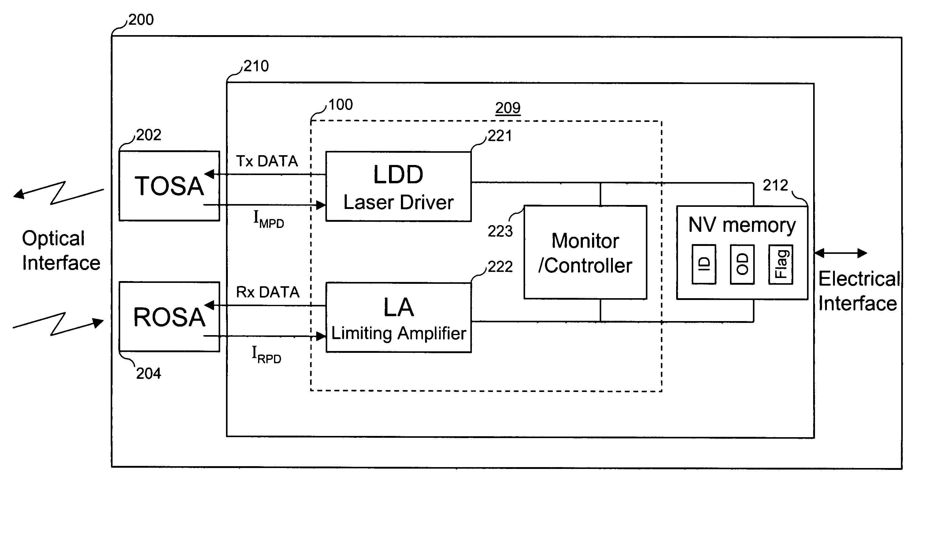
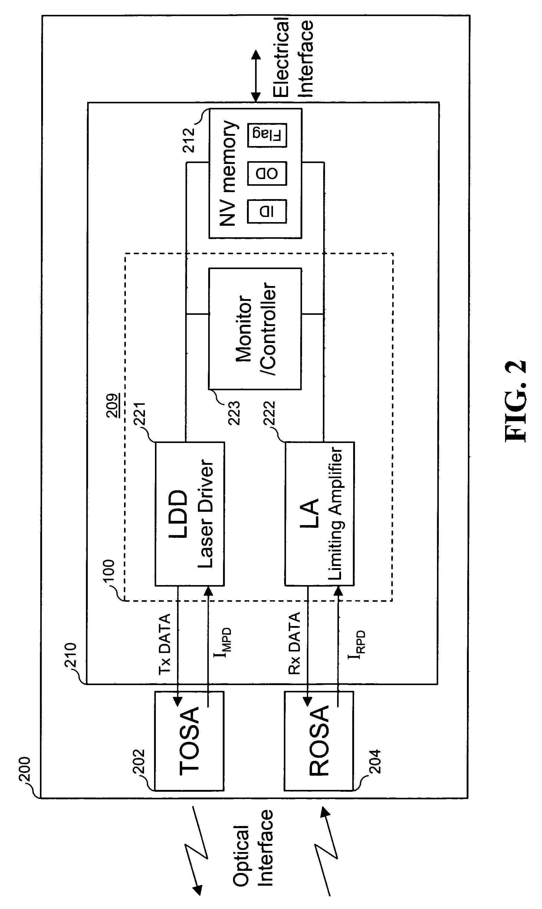
[0036]There is a continuous push in the industry for higher integration, denser port counts, lower power consumption, and lower component cost. It is therefore the purpose of this invention to integrate the typical separate integrated circuit chips, such as the laser driver, limiting amplifier and micro-controller, into a single integrated circuit chip to simplify the design and manufacturing, and thus reduce the cost of the optical transceivers. It is further the purpose of this invention to reduce the power consumption of the optical tran...


PUM


Abstract

An optical transceiver includes a single integrated circuit chip to integrate the drive, receive, control, and monitoring functions of the optical transceiver. The single chip may further have an advance replacement algorithm and monitoring algorithm for the opto-electronic devices of the optical transmitter and receiver to generate flags and / or an advance replacement indication. Methods, apparatus, and systems are disclosed.

Description

FIELD OF THE INVENTION[0001]This invention relates generally to optical transceivers. More particularly, the invention relates to integrated drive, receive, control and monitoring for optical transceivers.BACKGROUND OF THE INVENTION[0002]Optical transceivers are used in optical communications systems to convert data from electronics format into optical format and vice versa. A typical optical transceiver comprises a number of separate optical, optical-electrical, and electrical components including a semiconductor laser (LD) or light emitting diode (LED), an LD or LED driver IC, a P-I-N photodiode or Avalanche Photodiode (APD), a trans-impedance amplifier (TIA) and a limiting amplifier (LA). An LD can be a Fabry-Perot (FP) laser, a distributed feedback (DFB) laser, or a vertical cavity surface emitting laser (VCSEL). An LED can be either an edge emitting type or a surface emitting type of LED. These are discrete devices typically packaged separately in device packages, such as a thi...

Claims


Application Information

Patent Timeline
Patent Type & Authority Patents(United States)
IPC IPC(8): H04B10/24
CPCH04B10/40
Inventor CHIANG, MIN-WENJIANG, WENBINLEWIS, DAVID K.LEE, HSING-CHUNG
Owner NASA
Why Eureka
Try Eureka