Semiconductor device and method of manufacturing the same

a semiconductor chip and semiconductor technology, applied in the details of semiconductor/solid-state devices, semiconductor devices, electrical appliances, etc., can solve the problems of difficult filling control of resin for sealing semiconductor chips, device having power transistors, and possible corrosion

Inactive Publication Date: 2007-05-22
RENESAS ELECTRONICS CORP
View PDF5 Cites 22 Cited by
  • Summary
  • Abstract
  • Description
  • Claims
  • Application Information

AI Technical Summary

Benefits of technology

[0019]Advantageous effects obtained from the typical one of the inventions disclosed in the application is briefly described as follows.
[0020]That is, the metal plate terminal is provided on the electrode on the surface, which faces the mounting board, of the semiconductor chip housed in the recess of the metal cap via the connection material, and the semiconductor chip is sealed by the resin sealing body such that the metal plate terminal is exposed, thereby in the semiconductor device having the power transistor, the semiconductor chip can be sealed by resin without covering the electrode of the semiconductor device.
[0021]Moreover, the metal plate terminal is provided on the electrode on the surface, which faces the mounting board, of the semiconductor chip housed in the recess of the metal cap via the connection material, thereby the electrode configuration of the semiconductor device having the power transistor can be provided with versatility.
[0022]The metal plate terminal is provided on the electrode on the surface, which faces the mounting board, of the semiconductor chip housed in the recess of the metal cap via the connection material, thereby the thermal fatigue life of the connection portion between the semiconductor device having the power transistor and the mounting board can be improved.

Problems solved by technology

However, the inventors found that the semiconductor device having the power transistor had the following problems.
That is, first, there is a problem that filling control of the resin for sealing the semiconductor chip is difficult.
When a surface of the semiconductor chip is exposed, a problem on environmental-stress resistance such as leakage defect (particularly, area short at the outer circumferential portion of the semiconductor chip) or corrosion may occur.
Therefore, the semiconductor chip is preferably sealed by resin, however, when the semiconductor chip as a whole is covered with resin, the resin may concernedly cover surfaces of source and gate electrodes of the semiconductor chip, or contaminate them, and therefore filling control of resin for sealing the semiconductor chip, or control of a surface level of the resin is difficult, and actually only a limited area of side faces and the like of the semiconductor chip can be covered.
Since reduction in thickness of package tends to be further advanced hereinafter, such a problem will be increasingly significant.
Second, there is a problem that outer terminals for a gate and a source of the semiconductor device vary depending on chip size of the semiconductor chip, or positions or size of the gate and source electrodes of the semiconductor chip.
Third, there is a problem that since the semiconductor chip is directly connected to a mounting board having larger heat conductivity than the semiconductor chip, a connection portion for connecting the source and gate electrodes of the semiconductor chip to electrodes of the mounting board is applied with large thermal stress, and therefore thermal fatigue occurs early in the connection portion, consequently the connection portion is broken.

Method used


Image

  • Semiconductor device and method of manufacturing the same
  • Semiconductor device and method of manufacturing the same
  • Semiconductor device and method of manufacturing the same

Examples


embodiment 1

[Embodiment 1]

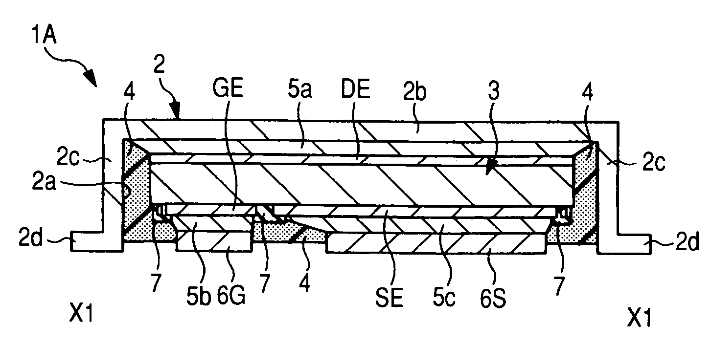
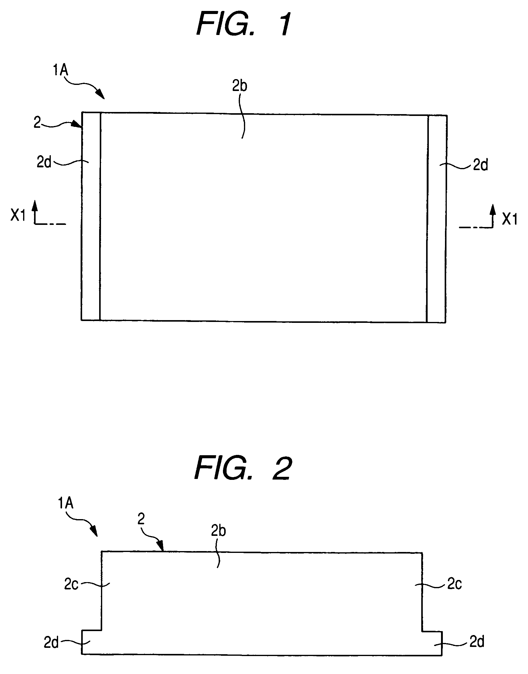
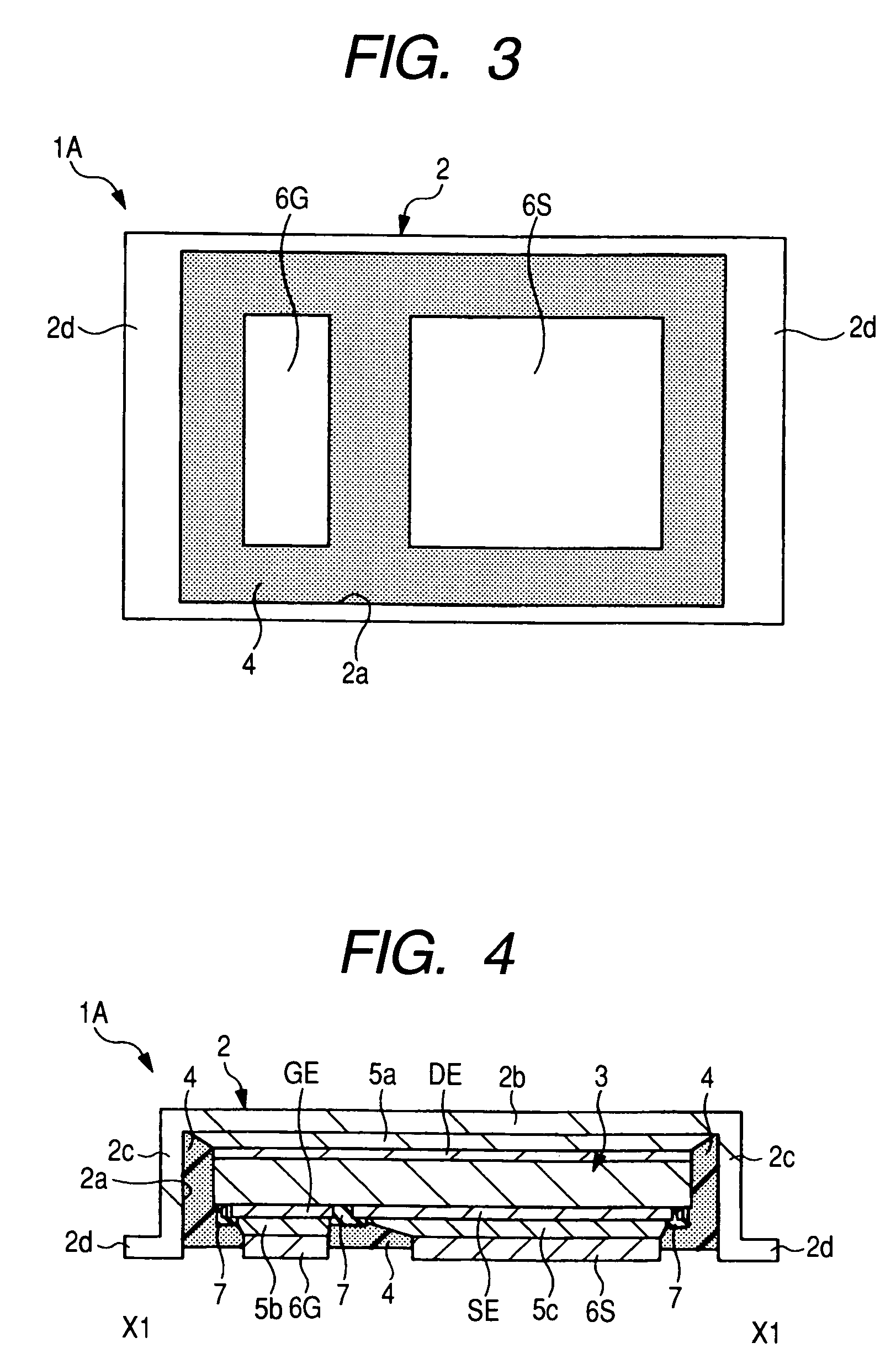
[0062]FIG. 1 is a plan view of a top of a semiconductor device of embodiment 1, FIG. 2 is a side view of the semiconductor device of FIG. 1, FIG. 3 is a plan view of a bottom of the semiconductor device of FIG. 1, and FIG. 4 is a cross section view along a line X1—X1 of the semiconductor device of FIG. 1.

[0063]The semiconductor device 1A of the embodiment 1 has a metal cap (conductive cap) 2, semiconductor chip 3 housed in a recess 2a of the metal cap 2, and resin sealing body 4 for sealing the semiconductor chip 3 filled in the recess 2a of the metal cap 2.

[0064]The metal cap 2 comprises a metal having excellent electric conductivity, heat conductivity, and machinability such as copper or copper alloys, and an exposed surface of it is applied with metal plating such as palladium (Pd) plating, lead (Pb)-tin (Sn) plating, tin-silver (Ag)-copper plating, or tin plating. The metal cap 2 integrally has a first part (upper part) 2b, second part (side part) 2c, and third par...

embodiment 2

(Embodiment 2)

[0119]FIG. 20 is a plan view of a top of a semiconductor device of the embodiment 2, FIG. 21 is a side view of the semiconductor device of FIG. 20, FIG. 22 is a plan view of a bottom of the semiconductor device of FIG. 20, FIG. 23 is a cross section view along a line X5—X5 of the semiconductor device of FIG. 20, and FIG. 24 is a cross section view along a line Y1—Y1 of the semiconductor device of FIG. 20.

[0120]In the semiconductor device 1B of the embodiment 2, a shallow recess 2e extending in a direction of the first part (head and upper part) is formed at lower parts of side faces of both longitudinal sides of the metal cap 2, and the metal plate terminals 6G, 6S extend long along a narrow direction of the metal cap 2 compared with the case of the embodiment 1, and respective two ends of them in the extending direction are protruded (exposed) outside of the metal cap 2 through respective recesses 2e at the lower parts of the side faces of both the longitudinal sides ...

embodiment 3

(Embodiment 3)

[0131]FIG. 31 is a plan view of a top of a semiconductor device of the embodiment 3, FIG. 32 is a side view of the semiconductor device of FIG. 31, and FIG. 33 is a plan view of a bottom of the semiconductor device of FIG. 31. A cross section view along a line X5—X5 of FIG. 31 is equal to that of FIG. 23, and a cross section view along a line Y1—Y1 of FIG. 31 is equal to that of FIG. 24.

[0132]A semiconductor device 1C in the embodiment 3 is approximately equal to that of the embodiment 2. It differs in that the lead portions 6G2, 6S2 of the metal plate terminals 6G, 6S is small in width compared with the body portions 6G1, 6S1. The metal plate terminal 6S has a plurality of lead portions 6S2 that extend from one body portion 6S1, and is generally formed into a comblike shape. A mounting condition of the semiconductor device 1C is not different from that described in the embodiment 2 except for smaller width of the lead portions 6G2, 6S2, therefore diagrammatic represen...


PUM


Abstract

A semiconductor chip is sealed by resin without covering an outer terminal of a semiconductor device having a power transistor. A semiconductor chip having a power transistor is housed within a recess of a metal cap while a drain electrode on a first surface of the semiconductor chip is bonded to a bottom of the recess via a connection material. A gate electrode and a source electrode are formed on a second surface opposite to the first surface of the semiconductor chip, and the gate electrode and the source electrode are bonded with metal plate terminals. In addition, the semiconductor chip is sealed by a resin sealing body with mounting-surfaces of the metal plate terminals being exposed. Mounting surfaces of the metal plate terminals and a third part of the metal cap are bonded to electrodes on a mounting board.

Description

BACKGROUND OF THE INVENTION[0001]1. Field of the Invention[0002]The present invention relates to a semiconductor device and a method for manufacturing the device, particularly relates to a packaging technique of a semiconductor device having a power transistor.[0003]2. Description of Related Art[0004]A high-power semiconductor device includes a semiconductor device having a semiconductor chip in which a power transistor such as power MOSFET (Metal Oxide Semiconductor Field-Effect-Transistor), IGBT (Insulated Gate Bipolar Transistor), and bipolar power transistor is formed.[0005]The semiconductor device having such a power transistor is described in, for example, International Patent Application No. W2001 / 075961 (patent literature 1) which discloses a structure of a semiconductor device having the power MOS FET. The paragraph 0024 and FIG. 21 of the patent literature 1 disclose a configuration in which a drain electrode of a die (semiconductor chip) is connected to a surface of an in...

Claims


Application Information

Patent Timeline
Patent Type & Authority Patents(United States)
IPC IPC(8): H01L21/44H01L21/48
CPCH01L21/52H01L23/24H01L23/488H01L23/49562H01L24/34H01L2924/1305H01L2924/12032H01L2924/1306H01L2224/16245H01L2224/73253H01L2224/16H01L2224/73153H01L2924/01013H01L2924/01029H01L2924/0103H01L2924/01032H01L2924/01046H01L2924/01049H01L2924/01078H01L2924/01079H01L2924/01082H01L2924/13055H01L2924/13091H01L2924/01005H01L2924/01006H01L2924/01023H01L2924/01033H01L2924/01047H01L2924/01074H01L2224/32245H01L2924/00H01L2924/351H01L2924/181H01L2224/40225H01L24/40H01L2224/0558H01L2224/05573H01L2224/05568H01L2224/05155H01L2224/05166H01L2224/05624H01L2224/05644H01L2224/84801H01L2224/83801H01L2224/8385H01L2224/8485H01L24/05H01L2224/0603H01L24/84H01L2224/06181H01L2924/00014H01L24/36
Inventor KAGII, HIDEMASAMUTO, AKIRASHIMIZU, ICHIOARAI, KATSUOSATO, HIROSHINAKAMURA, HIROYUKIOSAKA, MASAHIKONAKAJO, TAKUYAOKAWA, KEIICHIOKA, HIROI
Owner RENESAS ELECTRONICS CORP
Why Eureka
Try Eureka