

Faraday shield disposed within an inductively coupled plasma etching apparatus
a plasma etching and inductively coupled technology, applied in the field of semiconductor fabrication, can solve the problems of affecting the etching process, interfering with the etching process, and not necessarily uniform field, and achieve the effect of preventing the erosion of the etching chamber window
- Summary
- Abstract
- Description
- Claims
- Application Information
AI Technical Summary
Benefits of technology
Problems solved by technology
Method used
Image

Examples
Embodiment Construction
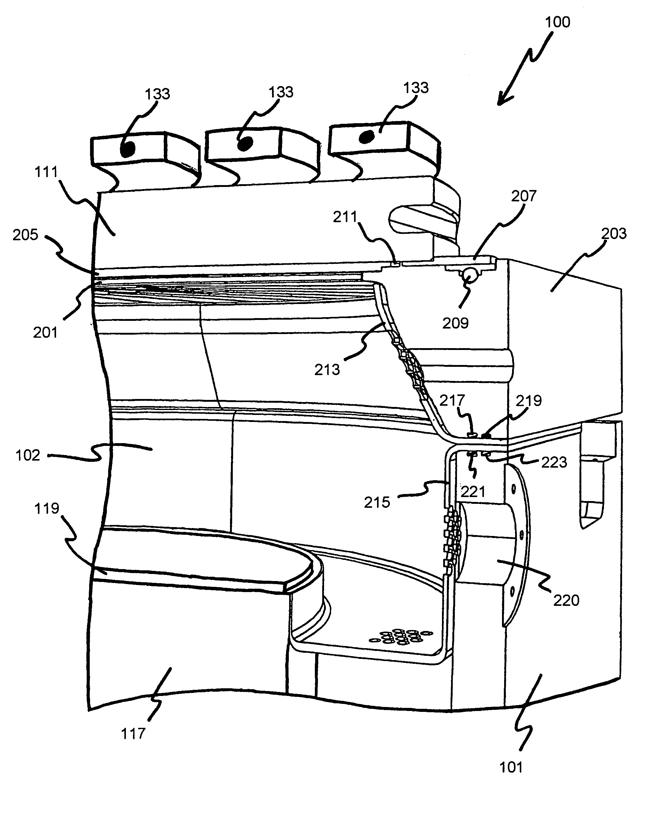
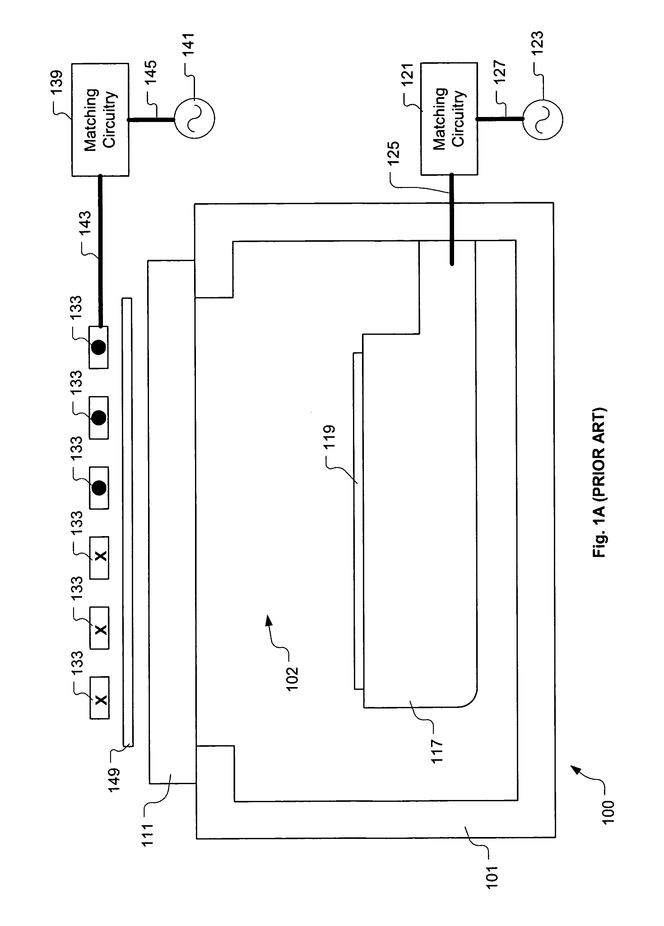
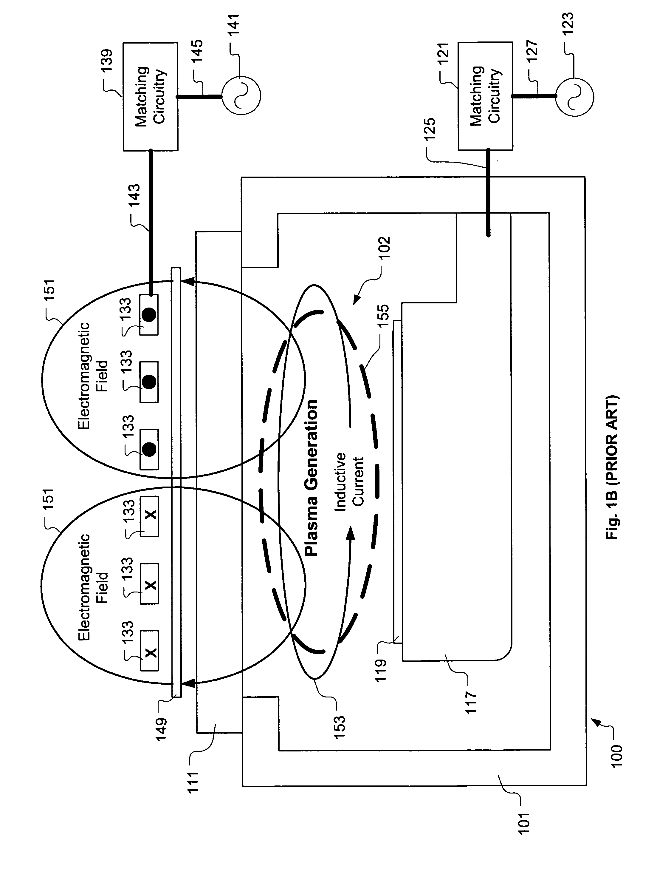
[0045]An invention is disclosed for apparatuses and methods for positioning and using a Faraday shield in direct exposure to a plasma within an inductively coupled plasma etching apparatus. Broadly speaking, the present invention maintains a condition of an etching chamber window. Configuring the Faraday shield between the window and the plasma prevents erosion of the window resulting from plasma sputter and shunts heat generated by an etching process away from the window. The present invention solves one problem of the prior art by reducing the window replacement frequency driven by erosion of the window due to plasma sputter. The present invention solves another problem of the prior art by allowing the use of a larger variety of window materials through a relaxation of thermal performance requirements afforded by the shunting of heat away from the window.
[0046]In the following description, numerous specific details are set forth in order to provide a thorough understanding of the ...
PUM
| Property | Measurement | Unit |
|---|---|---|
| Length | aaaaa | aaaaa |
| Length | aaaaa | aaaaa |
| Thickness | aaaaa | aaaaa |
Abstract
Description
Claims
Application Information