Dummy structures extending from seal ring into active circuit area of integrated circuit chip

a technology of integrated circuit chip and active circuit area, which is applied in the direction of electrical apparatus, semiconductor devices, semiconductor/solid-state device details, etc., can solve the problems of not allowing metal wiring circuitry and semiconductor devices to pass under or be located below the bond pad structure, many low-k dielectric materials are highly susceptible to cracking or lack the strength needed to withstand some mechanical processes, peeling or delamination, etc., to achieve the effect of reducing the area of dielectric material

Active Publication Date: 2007-05-29
TAIWAN SEMICON MFG CO LTD
View PDF12 Cites 20 Cited by
  • Summary
  • Abstract
  • Description
  • Claims
  • Application Information

AI Technical Summary

Problems solved by technology

Prior bond pad structures were fabricated from the bottom to the top layers, which did not allow metal wiring circuitry and semiconductor devices to pass under or be located below the bond pad structure.
Hence, many low-k dielectric materials are highly susceptible to cracking or lack strength needed to withstand some mechanical processes (e.g., wire bonding, CMP).
Not only do low-k dielectric materials tend to be relatively weak in compression strength, they also tend to be weak in adhesion strength and shearing strength, which can cause peeling or delamination.
These forces may cause cracking in the relatively weak low-k dielectric layers.
These forces may cause peeling or dislocation of the bond pad structure.
Such stresses can also cause cracking, peeling, delamination, or even relatively large chunks of the chip to be removed.
At the same time, the extensive use of low-k dielectric materials has greatly weakened the IMD layers, which calls for wider streets.

Method used


Image

  • Dummy structures extending from seal ring into active circuit area of integrated circuit chip
  • Dummy structures extending from seal ring into active circuit area of integrated circuit chip
  • Dummy structures extending from seal ring into active circuit area of integrated circuit chip

Examples


Embodiment Construction

[0015]Referring now to the drawings, wherein like reference numbers are used herein to designate like or similar elements throughout the various views, illustrative embodiments of the present invention are shown and described. The figures are not necessarily drawn to scale, and in some instances the drawings have been exaggerated and / or simplified in places for illustrative purposes only. One of ordinary skill in the art will appreciate the many possible applications and variations of the present invention based on the following illustrative embodiments of the present invention.

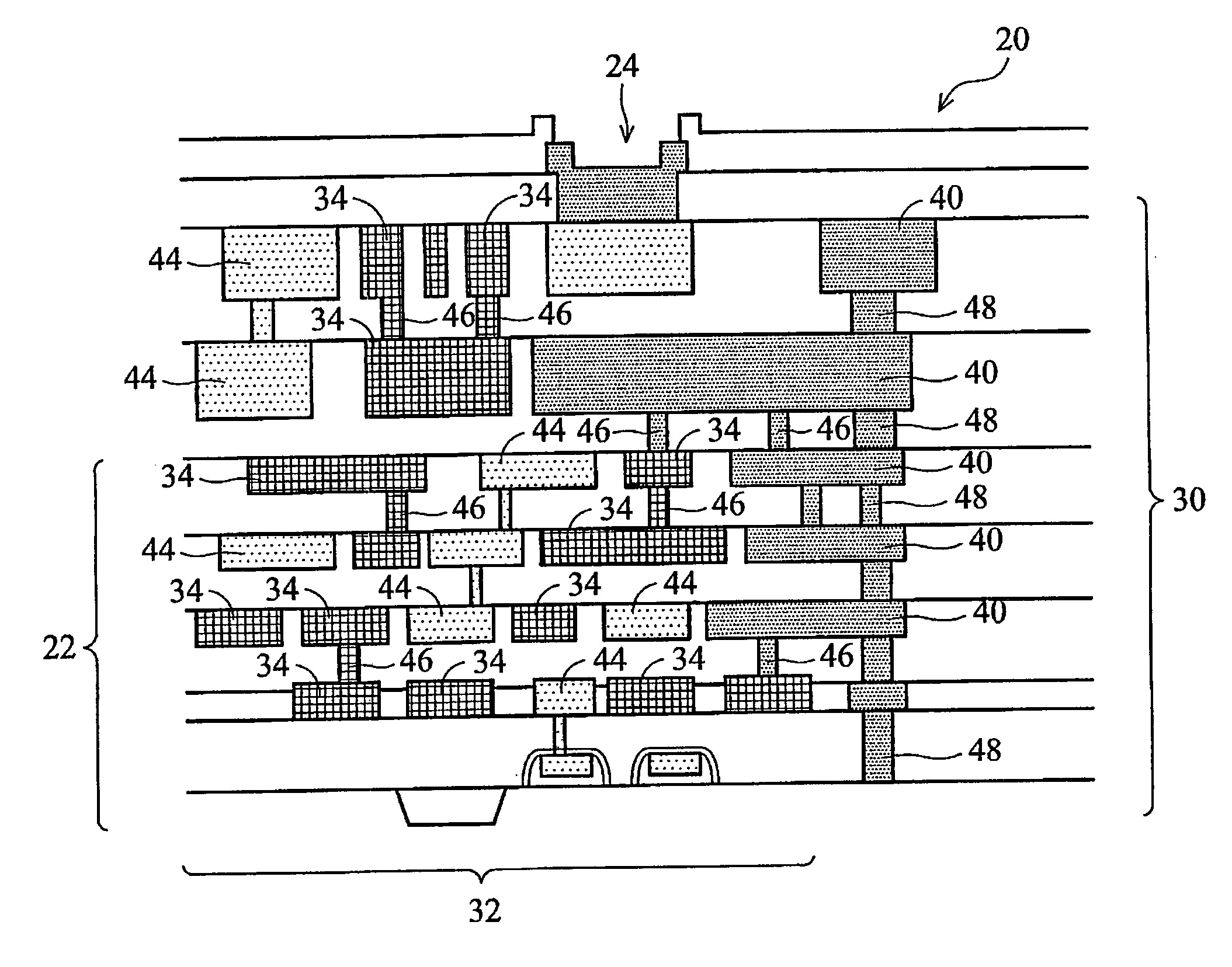
[0016]FIG. 1 is a cross-section view showing a portion of an integrated circuit chip. The chip 20 of FIG. 1 has portions of active circuits (of an integrated circuit) 22 formed under the bond pads 24. As illustrated in FIG. 1, part of a seal ring 30 is shown, which extends about the perimeter of the chip 20 around the active area(s) 32. Also, FIG. 1 shows example dummy structures 34 dispersed throughout the a...


PUM


Abstract

An integrated circuit chip is provided, which includes an active circuit area, a seal ring structure, and a first dummy structure. The seal ring structure is formed at least partially around the active circuit area. The first dummy structure extends from the seal ring structure into the active circuit area. Other dummy structures that are not directly joined to the seal ring structure at a given level may be provided also to further fill in spaces between active wiring. A software algorithm included in a layout tool may allow for automatically laying out such structures in accordance with predetermined layout design rules.

Description

TECHNICAL FIELD[0001]The present invention generally relates to dummy structures for mechanically strengthening an integrated circuit chip. More specifically, it relates to dummy structures extending from a seal ring into an active circuit area of an integrated circuit chip.BACKGROUND[0002]Integrated circuit (IC) chips are often electrically connected by wires (e.g., gold or aluminum wires) to a leadframe or a substrate in a packaging assembly to provide external signal exchange. Such wires are typically wire bonded to bond pads formed on an IC chip using thermal compression and / or ultrasonic vibration. A wire bonding process exerts thermal and mechanical stresses on a bond pad and on the underlying intermetal dielectric (IMD) layers and structure below the bond pad. The bond pad structure and IMD layers need to be able to sustain these stresses to ensure a good bonding of the wire and to prevent damage to the IC chip.[0003]Prior bond pad structures were fabricated from the bottom t...

Claims


Application Information

Patent Timeline
Patent Type & Authority Patents(United States)
IPC IPC(8): H01L23/48
CPCH01L23/562H01L23/585H01L24/05H01L2224/04042H01L2224/48666H01L2224/48647H01L2224/48624H01L2224/48784H01L2224/48766H01L2224/48747H01L2224/48724H01L2224/48684H01L2924/01033H01L2924/01019H01L2924/30105H01L2924/14H01L2924/01079H01L2924/01074H01L2924/01029H01L2924/01022H01L2924/01014H01L2924/01013H01L2224/45144H01L2224/45124H01L2224/05684H01L2224/05666H01L24/45H01L2224/02166H01L2224/05624H01L2224/05647H01L2924/00014H01L2924/00
Inventor CHEN, HSIEN-WEI
Owner TAIWAN SEMICON MFG CO LTD
Why Eureka
Try Eureka