Output drive circuit that accommodates variable supply voltages

a variable supply voltage and drive circuit technology, applied in the field of output controllers, can solve the problems of reducing the charging rate of output pads, and increasing the cost of dual oxide processes

Active Publication Date: 2007-05-29
INTEGRATED DEVICE TECH INC
View PDF7 Cites 28 Cited by
  • Summary
  • Abstract
  • Description
  • Claims
  • Application Information

AI Technical Summary

Benefits of technology

[0009]Some embodiments of an output driver circuit according to the present invention include a first transistor coupled between a power supply voltage and an output pad; a second transistor coupled between the first transistor and the output pad; a level shifter coupled between the first transistor and an input signal, the level shifter providing a signal to a gate of the first transistor; and a control circuit coupled to a gate of the second transistor, the control circuit providing a signal to the gate of the second transistor in response to the input signal and a supply voltage control signal. The level shifter and the control circuit are coupled to a voltage that is set to ground when the supply voltage control signal indicates a low supply voltage and is set to an intermediate voltage when the supply voltage control signal indicates a high supply voltage. In such an arrangement, the voltages applied across a gate oxide of the first transistor and a gate oxide of the second transistor do not exceed the low supply voltage. In some embodiments, a one-shot can be coupled to the voltage to momentarily ground the voltage in order to increase the charging rate of the output pad when the supply voltage control signal indicates the high supply voltage.

Problems solved by technology

These later reductions to one volt supply designs now require the added expense of a dual oxide process, for example an 80 Å process for device potentials of 3.3 volts and a 16 Å process for device potentials of 1.0 volts.
The lower device potentials can result in lower power consumption.
Application of voltages greater than the design specification for a particular gate oxide thickness can result in damage to the transistor.
Further, application of high voltage power supplies in circuits that are formed with lower voltage transistors can affect the timing of those circuits.

Method used


Image

  • Output drive circuit that accommodates variable supply voltages
  • Output drive circuit that accommodates variable supply voltages
  • Output drive circuit that accommodates variable supply voltages

Examples


Embodiment Construction

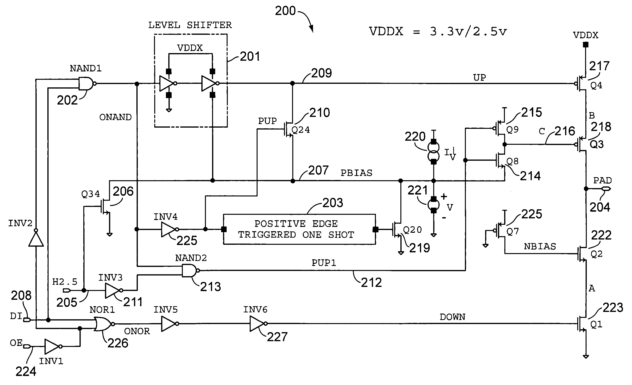
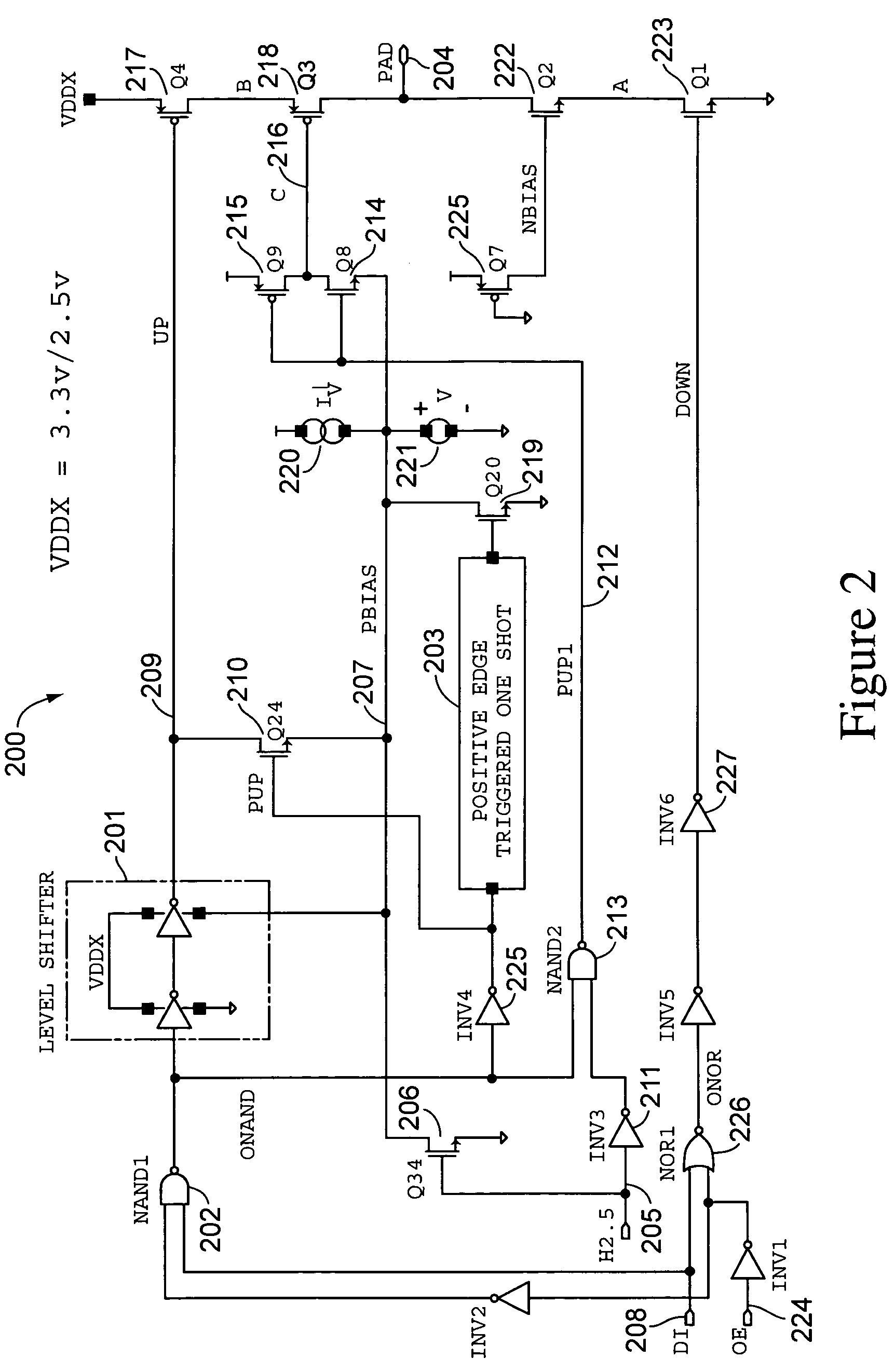
[0021]In accordance with the present invention, a driver circuit is presented that can operate with a low supply voltage or a high supply voltage. The transistors of the circuit can withstand application of the low supply voltage but may be damaged by direct application of the high supply voltage.

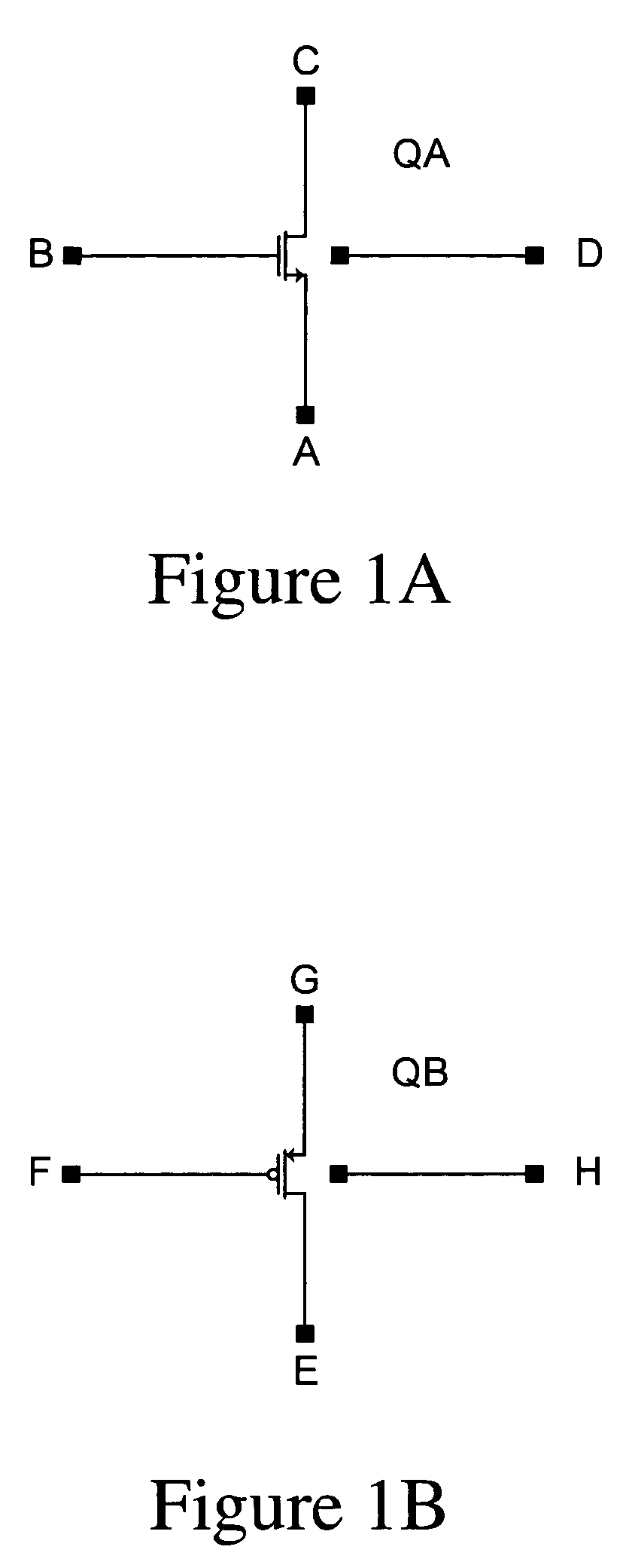
[0022]Embodiments of a driver circuit according to the present invention can meet at least two design objectives. First, the transistors processed with thin gate oxides should not exceed specified design limits in the high voltage environment (i.e., upon application of the high voltage power supply). Second, the delays of the circuit should be the same for both high and low voltage output drivers. FIGS. 1A and 1B illustrate the first design objective. FIG. 1A illustrates an N-channel transistor where the labels A, B, C, and D denote the source, gate, drain, and substrate nodes, respectively. FIG. 1B illustrates a P-channel transistor where E, F, G, and H denote the source, gate, drain, and ...


PUM


Abstract

In accordance with the invention, a driver circuit is described that permits a single thin gate oxide process to be utilized where a dual oxide process may normally be necessary. Circuits employing only thin gate oxide devices are used as the design basis for a single product with a single set of tooling and manufacturing process to operate within the same timing specifications for a core voltage output drive as well as for a higher system drive.

Description

RELATED APPLICATIONS[0001]The present application is related to and claims priority from U.S. Provisional Application 60 / 529,411, “Output Drive Circuit Which Tolerates Variable Supply Voltages,” filed on Dec. 11, 2003, by David Pilling, Leo Lee, and Mario Au, which is herein incorporated by reference in its entirety.BACKGROUND[0002]1. Field of the Invention[0003]The present invention relates to an output controller and, in particular, an output driver that accommodates variable supply voltages.[0004]2. Discussion of Related Art[0005]Circuit development is often a result of technological change. In the 1960's the N-channel MOS gate oxide thicknesses were about 2000 Å in order to support gate bias potentials of about 18 volts. In the last ten years, products that were designed with 130 Å thick gates for five volt supplies are now designed for operating supply voltages of 3.3 volts with core supplies of 2.5 volts. More recent designs with core voltages of 1.0 volts have 3.3 volt extern...

Claims


Application Information

Patent Timeline
Patent Type & Authority Patents(United States)
IPC IPC(8): H03B1/00H03K3/00H03K19/003H03K19/017H03K19/0185
CPCH03K19/00315H03K19/018585H03K19/01707
Inventor PILLING, DAVIDLEE, KAR-CHUNG LEOAU, MARIO FULAM
Owner INTEGRATED DEVICE TECH INC
Why Eureka
Try Eureka