Mounting structure in integrated circuit module

a technology of integrated circuit module and mounting structure, which is applied in the direction of sustainable manufacturing/processing, instruments, final product manufacturing, etc., can solve the problems of large memory chip or package, insufficient improvement in memory device technology, and difficulty in etc., and achieve the effect of mounting a plurality of chips or packages

Inactive Publication Date: 2007-06-05
SAMSUNG ELECTRONICS CO LTD
View PDF7 Cites 8 Cited by
  • Summary
  • Abstract
  • Description
  • Claims
  • Application Information

AI Technical Summary

Benefits of technology

[0012]Example embodiments of the present invention may provide an integrated circuit module, and a structure thereof, to effectively mount a plurality of packages in a limited space. In an embodiment, packages may be mounted with conventional form factors. Packages may also be mounted with bigger integrated circuit packages. Embodiments may mount ball grid array (BGA) type semiconductor memory packages with high-density. Further, an embodiment can mount bigger packages on an existing wiring board without reducing the number of packages.
[0013]Further, example embodiments may provide an improved memory card structure, a memory module mounting structure, and methods thereof, allowing three-dimensional mounting of memory chips of increased size on a wiring board. Example embodiments allow previous mounting methods without changing wiring boards, even when memory chips or packages increase in size and subsequently return to previous sizes.
[0016]Accordingly, in a structure and mounting method of an integrated circuit module, there are advantages of effectively mounting a plurality of chips or packages in a limited space without changing form factors. Furthermore, the plurality of chips may be mounted in such fashion even when the integrated circuit chip or package increases in size. Additionally, a structure and mounting method may be used even while mounting increased size packages on the wiring board without changing the number of packages. Likewise, the mounting method disclosed herein may easily change to a previously-applied mounting method without changing the wiring board, even when memory chip or package size increases and then again is reduced.

Problems solved by technology

However, as chips or packages in semiconductor memory devices become larger, difficulties arise in mounting a plurality of chips or packages on a board having a determined space.
However, improvements in memory device technology may not always be sufficient.
Memory devices often use general process technology, which can result in a relatively large memory chip or package.
As shown in the figure, it may be difficult or impossible for an integrated circuit module to contain all nine DRAM packages 21 on the wiring board 10.
Consequently, referring to FIG. 1b, a ninth package C9 may only be mounted by changing the memory module form factors, consequently causing compatibility and efficiency problems.
Previous approaches to improve mounting density of semiconductor integrated circuit packages prove insufficient.
However, the approach in Azuma is complicated, particularly in tiltably constructing an integrated circuit module through use of a supporting lead.
This problem is further complicated for BGA type memory packages.
Additionally, this need exists as integrated circuit packages increase in size.

Method used


Image

  • Mounting structure in integrated circuit module
  • Mounting structure in integrated circuit module
  • Mounting structure in integrated circuit module

Examples


Embodiment Construction

[0025]Embodiments of the present invention are more fully described below with reference to FIGS. 2 through 9 in which like components have been provided with like reference symbols and numerals. The present invention may, however, be embodied in many different forms and should not be construed as being limited to the example embodiments set forth herein. Rather, these embodiments are provided so that this disclosure is thorough and complete.

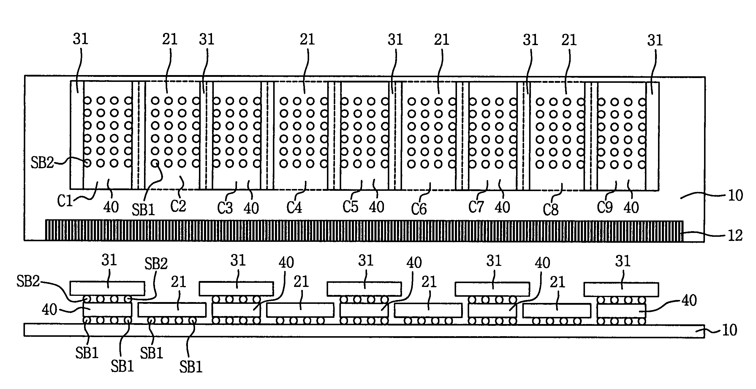
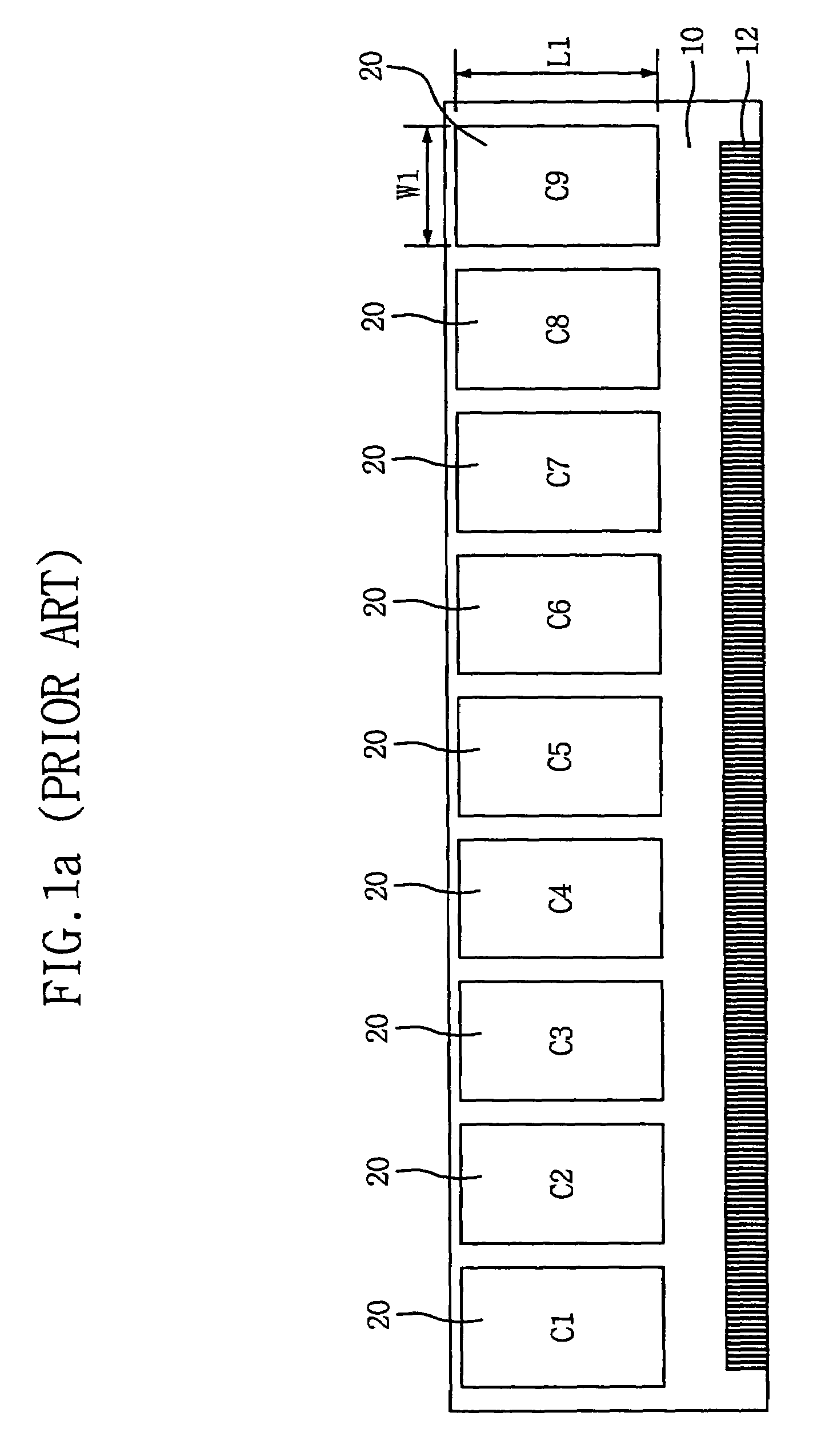
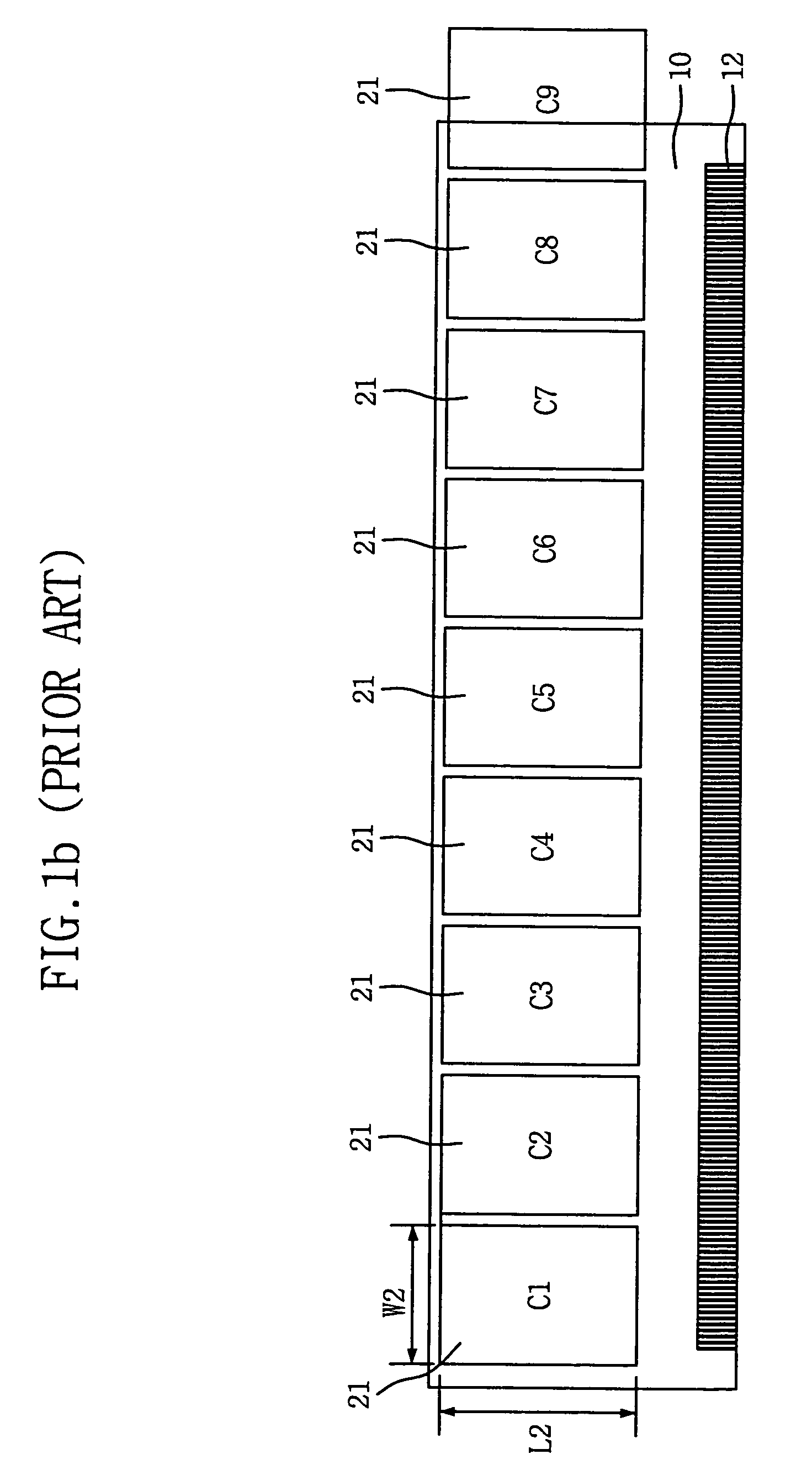
[0026]FIG. 2 is a plan view showing an embodiment mounting structure of an integrated circuit module. Referring to FIG. 2, the integrated circuit module includes a wiring board 10 which has a mounting space. The mounting space has a mounting length determined in a first direction as a long side direction, and a mounting width determined in a second direction as a short side direction, on at least one surface thereof. The wiring board also has a plurality of integrated circuit packages C1–C9 having a package mounting combination length longer tha...


PUM


Abstract

Embodiments of the present invention may include an integrated circuit module structure for a high-density mounting. An embodiment may include a wiring board, having a mounting space with a mounting length determined in a first direction and a mounting width determined in a second direction, on at least one surface thereof, and a plurality of integrated circuit packages having a package mounting combination length longer than the mounting length of the wiring board. An embodiment may also have some packages among the plurality of integrated circuit packages mounted directly on the mounting space, while other packages are mounted indirectly on the mounting space. The present embodiment may have packages that are overlapped horizontally and vertically distant from one another. Embodiments allow a plurality of chips or packages to be mounted in a limited area without changing a form factor of integrated circuit module even when integrated circuit chip or package size increases.

Description

CROSS REFERENCE TO RELATED APPLICATIONS[0001]This application claims priority from Korean Patent Application No. 2003-80105, filed on Nov. 13, 2003, the contents of which are incorporated herein by reference in their entirety.FIELD OF THE INVENTION[0002]The present invention relates to semiconductor device mounting, and more particularly, to an integrated circuit module for effectively mounting a plurality of semiconductor chips or a plurality of integrated circuit packages on a card or wiring board.PRIOR ART OF THE INVENTION[0003]Integrated circuit (IC) packages with encapsulated semiconductor chips are continually decreasing in size. Chip size packages (CSP) were recently developed having roughly the size of a bare chip.[0004]Users of electronic systems for communications or computing require continually higher performance, resulting in increasing needs for high-speed and high-integration in semiconductor memory devices such as DRAM (Dynamic Random Access Memory).[0005]As electron...

Claims


Application Information

Patent Timeline
Patent Type & Authority Patents(United States)
IPC IPC(8): H01L23/34H01L25/10G11C5/00H01L21/50H01L23/48H01L25/18H05K1/18
CPCH05K1/181H05K2201/097H05K2201/10378H05K2201/10515H01L2924/0002H05K2201/10734H01L2924/00Y02P70/50H01L23/48
Inventor CHO, JEONG-HYEONSO, BYUNG-SECHANG, JIN-KYU
Owner SAMSUNG ELECTRONICS CO LTD
Why Eureka
Try Eureka