

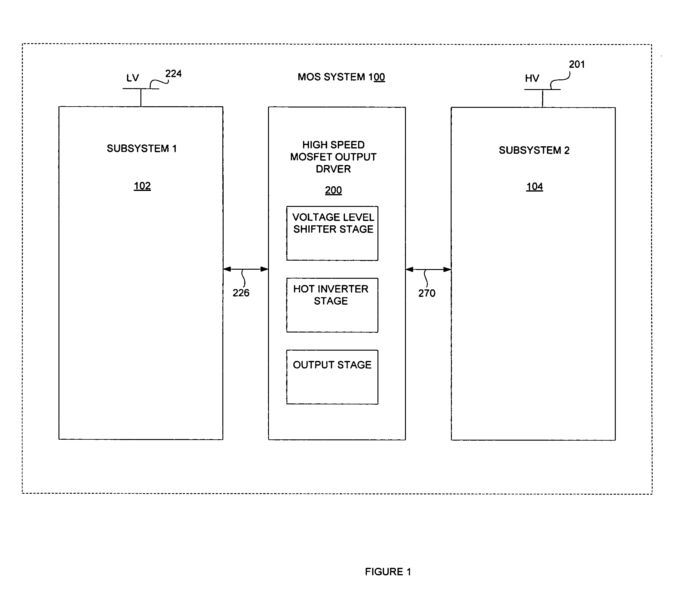
High speed MOSFET output driver
a high-speed, output driver technology, applied in the direction of pulse automatic control, pulse technique, reliability increasing modifications, etc., can solve the problems of low switching speed, low efficiency, and low efficiency of high-voltage output drivers with dual gate oxide components, so as to increase the voltage gain reduce and increase the minimum voltage level of the output signal
- Summary
- Abstract
- Description
- Claims
- Application Information
AI Technical Summary
Benefits of technology
Problems solved by technology
Method used
Image

Examples
Embodiment Construction
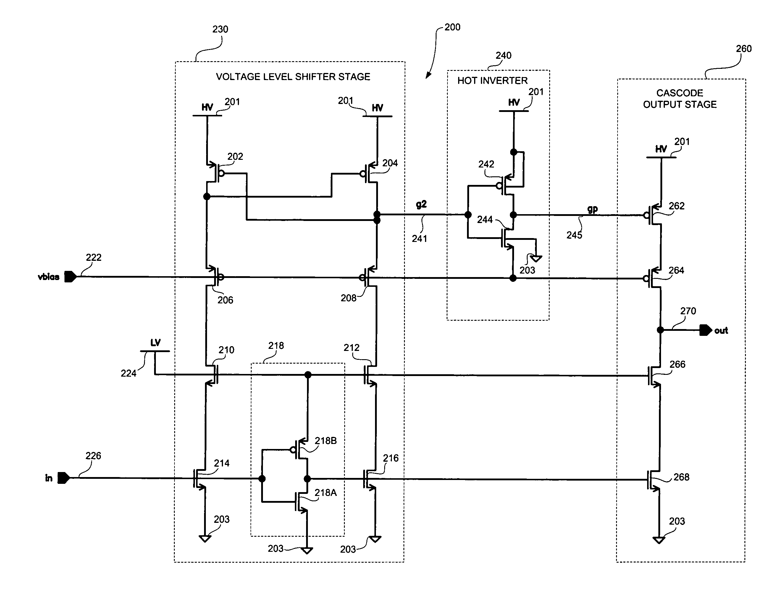
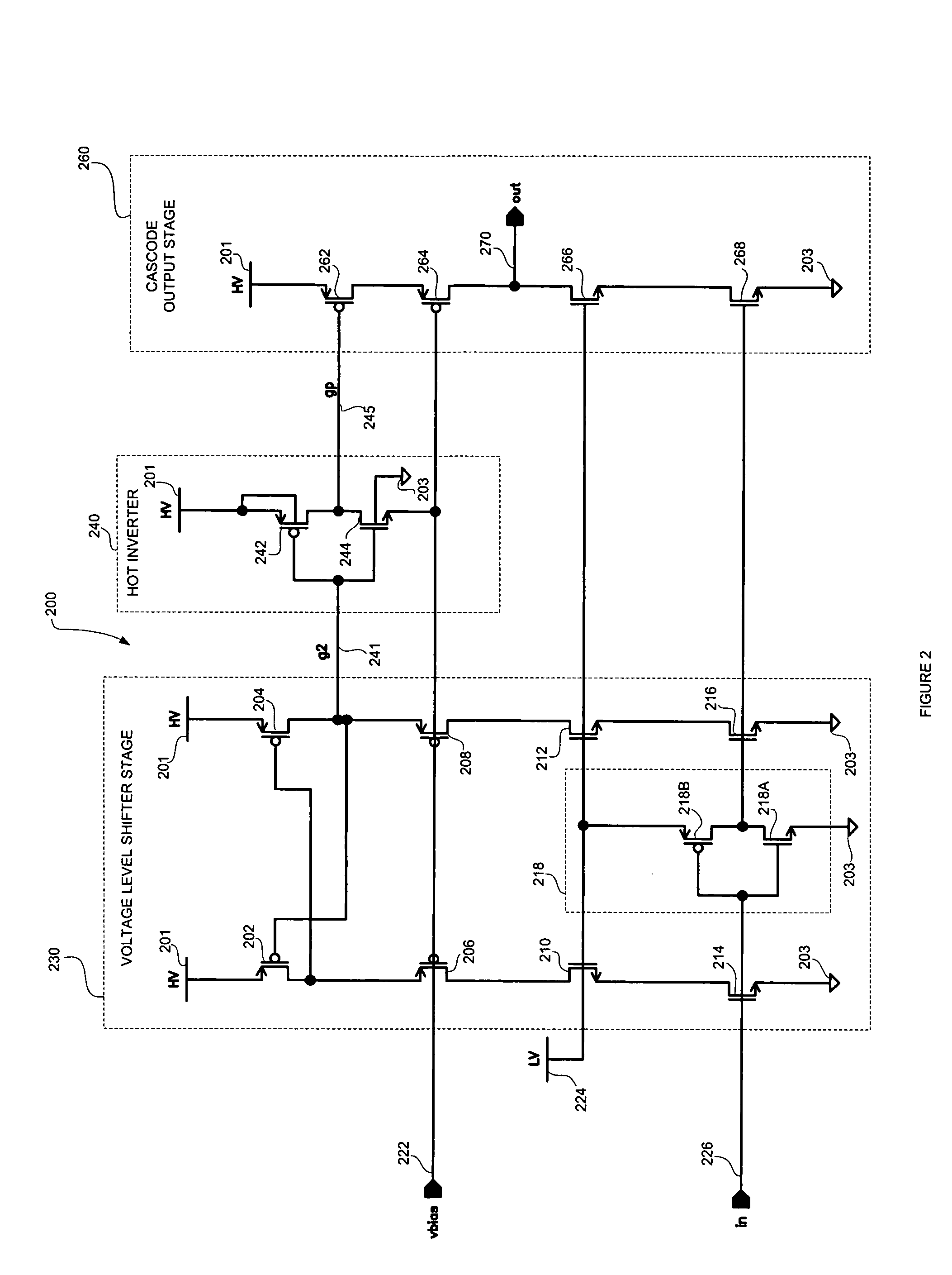
[0023]Reference will now be made in detail to the preferred embodiments of the invention, examples of which are illustrated in the accompanying drawings. While the invention will be described in conjunction with the preferred embodiments, it will be understood that they are not intended to limit the invention to these embodiments. On the contrary, the invention is intended to cover alternatives, modifications and equivalents, which may be included within the spirit and scope of the invention as defined by the appended claims. Furthermore, in the following detailed description of the present invention, numerous specific details are set forth in order to provide a thorough understanding of the present invention. However, it will be obvious to one of ordinary skill in the art that the present invention may be practiced without these specific details. In other instances, well-known methods, procedures, components, and circuits have not been described in detail so as not to unnecessarily...
PUM
 Abstract
Description
Claims
Application Information