Latch-type sense amplifier

a technology of latch-type sense amplifier and latch-type, which is applied in the direction of information storage, static storage, digital storage, etc., can solve the problems of capacitance imbalance, inability to provide reliable operation, and insufficient high reliability of conventional sense amplifiers, so as to reduce memory access times and high-speed memory cell operation

Active Publication Date: 2007-06-05
STMICROELECTRONICS PVT LTD
View PDF10 Cites 29 Cited by
  • Summary
  • Abstract
  • Description
  • Claims
  • Application Information

AI Technical Summary

Benefits of technology

[0008]The disclosed embodiments of the present invention overcome the drawbacks mentioned above and provide an improved sense amplifier that offers reliable sensing of low voltage differences thereby enabling high-speed memory cell operation and reducing the memory access times during a read operation.

Problems solved by technology

Conventional sense amplifiers are unable to provide reliable operation under these conditions.
The problem with this arrangement is that the split required for latching correct data with sufficiently high reliability is dependent on two important criteria—the threshold voltage mismatch between the NMOS sense transistors 30 and 40 in the latch, and the capacitance imbalance that may exist between the internal nodes (SN1& SN2) of the sense amplifier.
Triggering the sense amplifier at a voltage differential equal to the minimum required voltage results in large access times, which limits the speed of the device.
High-speed memory designs are not feasible with such an arrangement.
As the discharge rate is slow in high-density memories, even a few extra milli-volts of split result in an increase in the overall access time.
Triggering the sense amplifier at such a voltage split results in larger access times, which ultimately proves to be a bottleneck in high-speed memory designs.
A further disadvantage is that this type of sense amplifier is not very reliable when the voltage difference between the bit lines is small.
The disadvantage of the circuit described by this invention is that it is complex, involving more number of transistors, which require more signals to operate.
Coordination of the many signals used in this device is cumbersome.

Method used


Image

  • Latch-type sense amplifier
  • Latch-type sense amplifier
  • Latch-type sense amplifier

Examples


Embodiment Construction

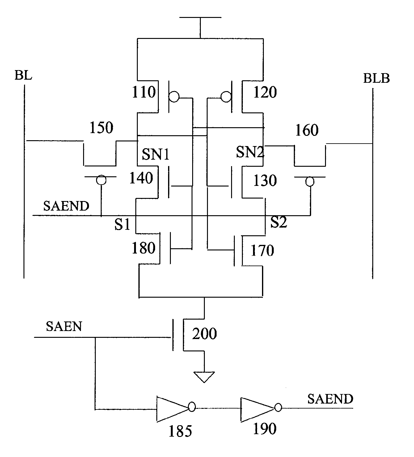
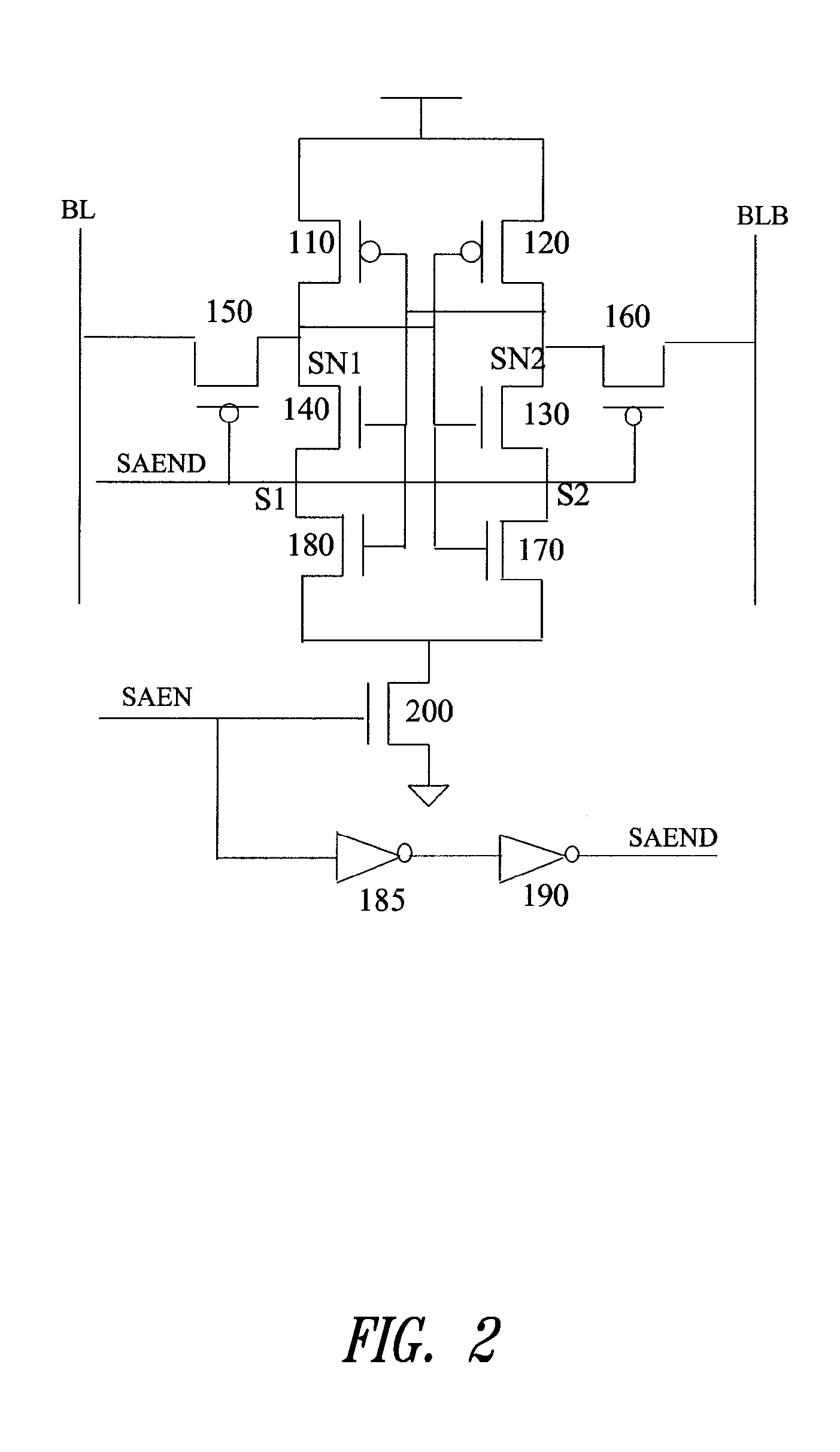
[0022]The disclosed embodiments of the present invention aim to overcome the above-mentioned problem of longer access times in memories by triggering the sense amplifier at a voltage split less than what is required in the conventional scheme. The improved circuit is able to achieve a substantial improvement of around 15–20% in reliability for sensing low voltages as compared to the conventional circuits. This improved reliability further results in achieving a significant access time improvement.

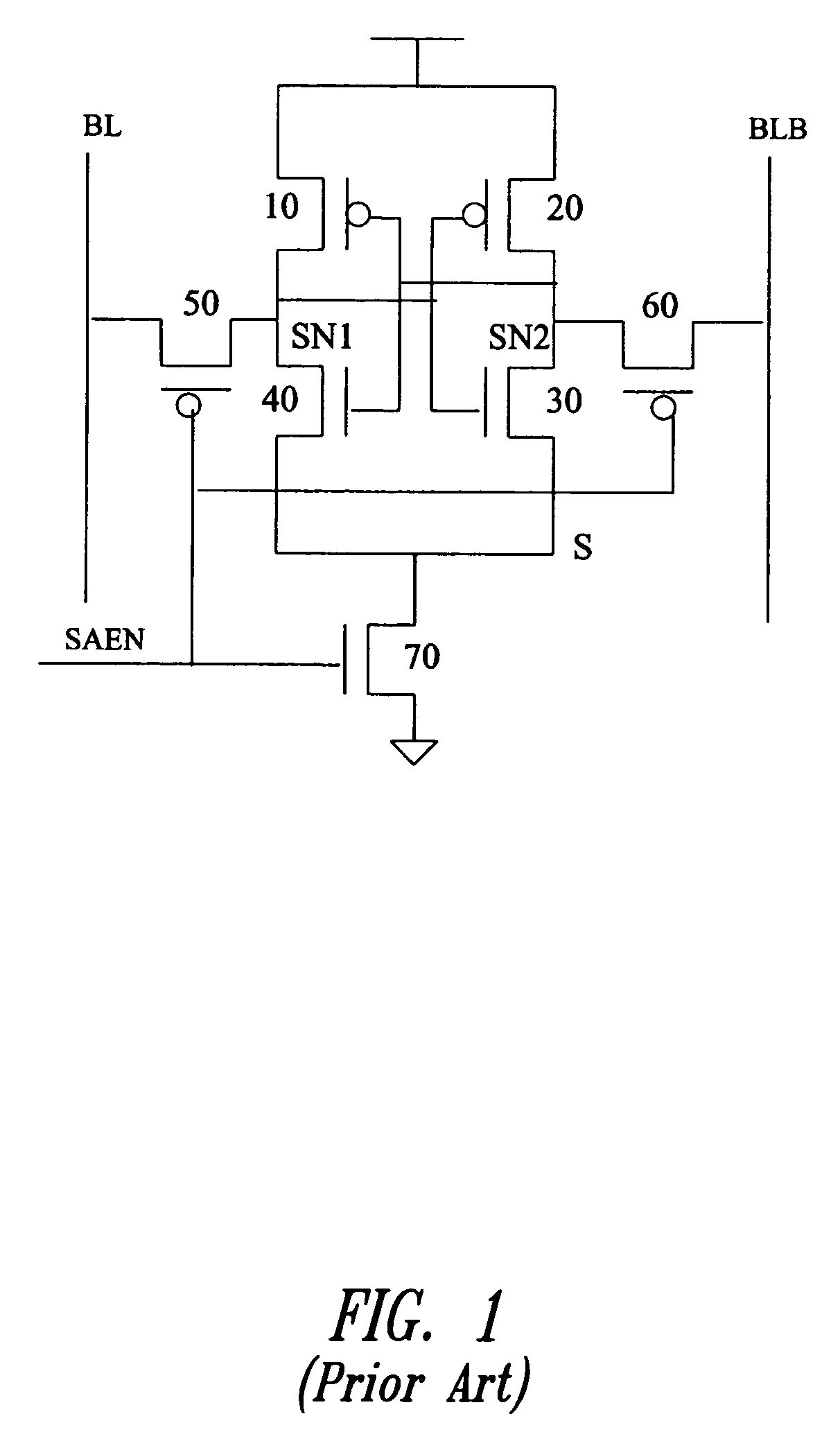
[0023]The circuit in FIG. 2 illustrates an improved latch-type sense amplifier as provided by the present invention. The circuit comprises a modified latch consisting of PMOS transistors 110, 120, NMOS transistors 130, 140, and an additional set of NMOS transistors 170, 180. The bit line BL is connected through a PMOS transistor 150 and the bit line BLB is connected through a PMOS transistor 160. The NMOS transistor 200, controlled by the SAEN signal, is used for coupling the latch to a sup...


PUM


Abstract

An improved latch-type sense amplifier circuit having two cross-coupled inverters forming a latch, a supply coupling device for selectively connecting the latch to a supply source, and a bit line coupling circuits for selectively connecting the inputs of each inverter to the complimentary bit line from the memory array. The circuit is configured to sense a voltage difference between the bit lines with improved reliability by providing a delayed sense amplifier enable signal to pass transistors for delaying disconnection of the bit lines from the sense amplifier until the latching action is completed, and adding two transistors in series with the existing transistors of the conventional latch for correcting the offset between the threshold voltages of the inverters of the latch.

Description

BACKGROUND OF THE INVENTION[0001]1. Field of the Invention[0002]The present invention relates in general to latch-type sense amplifiers and, more particularly, provides an improved apparatus for a latch-type sense amplifier for sensing low voltage splits with very high reliability.[0003]2. Description of the Related Art[0004]Sense amplifiers are used in memory devices for sensing the output voltage of selected memory cells. With advancements in technology, memory cells are continually shrinking in size. The reduction in memory cell size is accompanied by reduction in the sensed voltage from the memory cell. Conventional sense amplifiers are unable to provide reliable operation under these conditions.[0005]Consider the conventional latch-type sense amplifier of FIG. 1. PMOS transistor 10, PMOS transistor 20, NMOS transistor 30, and NMOS transistor 40 together form the memory latch. Bit line BL is connected through PMOS transistor 50 to the latch while complementary bit line BLB is co...

Claims


Application Information

Patent Timeline
Patent Type & Authority Patents(United States)
IPC IPC(8): G11C7/00G11C7/06
CPCG11C7/065
Inventor GUPTA, ANUJCHOPRA, SANJEEV
Owner STMICROELECTRONICS PVT LTD
Why Eureka
Try Eureka