
Method for evaluating photo mask and method for manufacturing semiconductor device

a technology for semiconductor devices and photo masks, applied in the direction of microlithography exposure devices, instruments, photomechanical treatment, etc., can solve the problems of failure of manufactured photo masks, poor manufacturing yield, and insufficient capacity to make a decision whether the photo mask is good or failur

Inactive Publication Date: 2007-06-12
KK TOSHIBA
View PDF5 Cites 6 Cited by
  • Summary
  • Abstract
  • Description
  • Claims
  • Application Information

AI Technical Summary

Benefits of technology

The present invention provides a method for evaluating a photo mask and a method for manufacturing a semiconductor device using the photo mask. The method involves preparing a photo mask with a unit drawing pattern and finding dimensional variations in the photo mask caused by positional displacement, size mismatch, etching, and development. The dimensional variations are then used to estimate the deteriorated exposure latitude of the photo mask, which is compared to an allowable level to determine the quality of the photo mask. This allows for the selection of a good photo mask for use in the manufacturing process, resulting in improved quality of the semiconductor device.

Problems solved by technology

If, therefore, even one of these checking items does not satisfy their specification, the manufactured photo mask is rejected as being failure.
Under such a stricter accuracy thus sought, a high accuracy manufacturing technique has been progressed, but the manufacturing yield is becoming poor.
However, this is not adequate as to make a decision whether the photomask is good or failure.
There is a risk that a good mask will be decided as being failure.
This involves a fall in manufacturing yield of photo masks, thus presenting a problem.
Therefore, there is a risk that a good photo mask will be decided as being an failure one.

Method used


Image

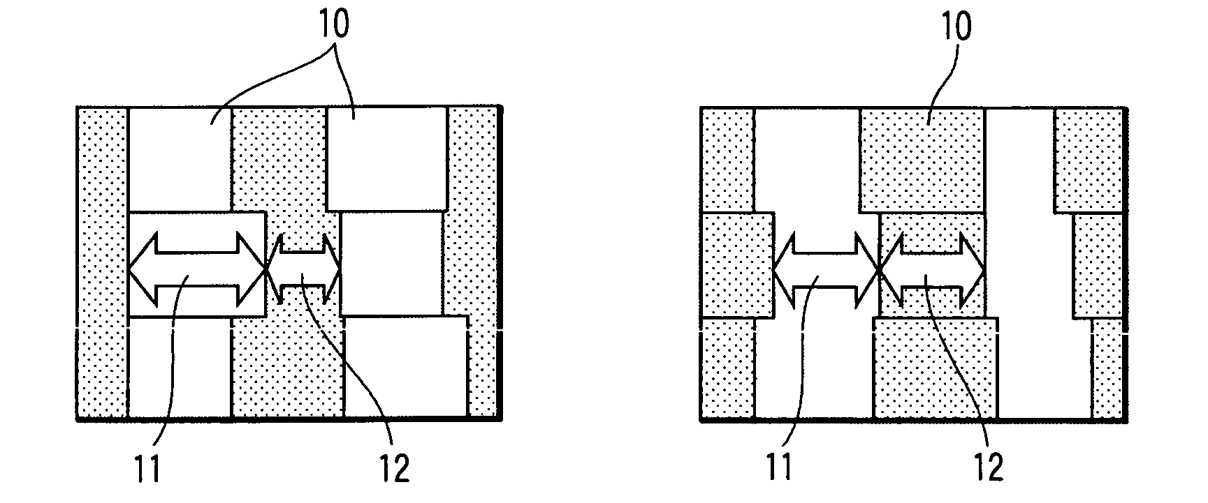
  • Method for evaluating photo mask and method for manufacturing semiconductor device
  • Method for evaluating photo mask and method for manufacturing semiconductor device
  • Method for evaluating photo mask and method for manufacturing semiconductor device

Examples


first embodiment

(First Embodiment)

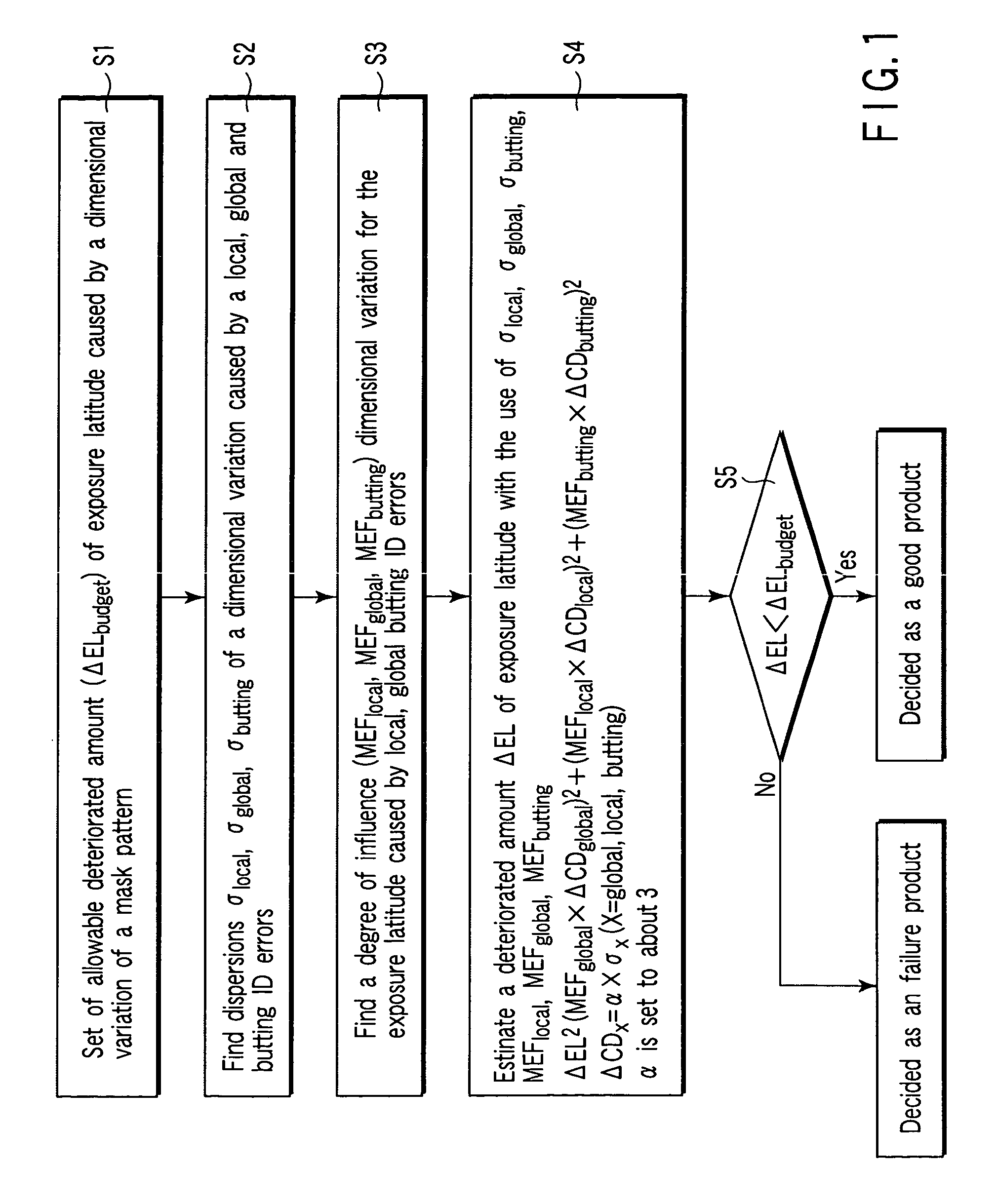
[0022]FIG. 1 is a flow chart showing a method of the evaluation of photo masks according to the first embodiment of the present invention.

[0023]First, a mask blanks is prepared. The mask blanks has a transparent substrate, such as a quartz substrate, and a light shielding film, such as a Cr film, on the transparent substrate.

[0024]Then a 130 nm-thick L / S pattern is formed over the mask blanks to provide a photo mask.

[0025]A concrete manufacturing method of the photo mask is as will be set out below.

[0026]A resist is coated on the mask blanks, an L / S pattern is drawn on the resist film with the use of an electron beam drawing device, and the resultant resist is developed to provide a resist pattern including the L / S pattern. Then the light shielding film is etched by using the resist pattern as a mask, thereafter the resist pattern is removed. By doing so, the photo mask is obtained which includes the L / S pattern. The mask blanks and photo masks are made by the same...

second embodiment

(Second Embodiment)

[0042]In this embodiment, the evaluation method of photo masks will be explained below and, according to the second method, a process (step S2) for finding the dispersion of a dimensional variation of the first embodiment can be simplified.

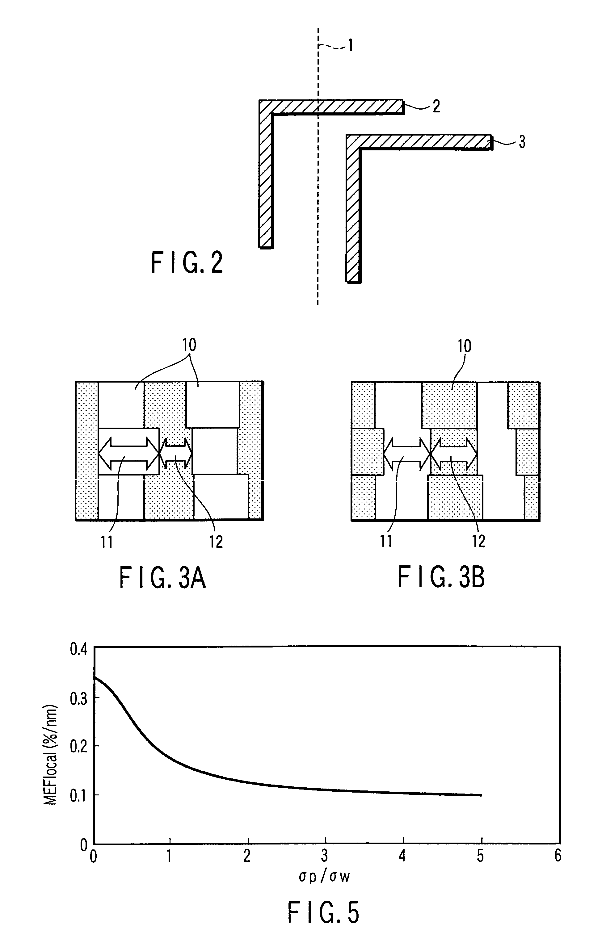
[0043]FIG. 2 is a plan view showing a pattern 2 extending across a boundary 1 between deflection areas and a pattern 3 not extending across the deflection areas. In the second embodiment, the pattern 3 not extending across the boundary between the deflection variation is treated as a target for measuring the dimensional variation. This method can be done without paying no consideration of any dimensional variation ΔCDbutting caused by the butting CD error.

[0044]However, no separation is made between a dimensional variation ΔCDlocal caused by a local CD error and a dimensional variation ΔCDglobal caused by a global CD error. From the standpoint of improving a throughput for measurement, it would be done without measurement for fi...

third embodiment

(Third Embodiment)

[0051]In the present embodiment, a method of finding a degree of influence MEFlocal by a simulation will be explained below. The method of finding the degree of influence MEFlocal can be applicable to the first and second embodiments. Since a manner how to apply the method to the first and second embodiments is evident, a detailed explanation of the manner is omitted in the present embodiment.

[0052]First, a positional displacement and size of a unit drawing pattern are measured, and a dispersion resulting from a dimensional variation caused by the positional displacement and size mismatch of the unit drawing pattern (local CD error). σprepresents the dispersion caused by the positional displacement of the unit drawing picture and σw represents the dispersion caused by the size mismatch of the unit drawing pattern.

[0053]The degree of influence, MEFlocal depends upon the dispersions σp and σw. The MEFlocal is found as a function of dispersions σp, σw by a Monte Carlo...


PUM

PropertyMeasurementUnit
sizeaaaaaaaaaa
areaaaaaaaaaaa
transmittivityaaaaaaaaaa

Abstract

A method for evaluating a photo mask comprises preparing a photo mask including a unit drawing pattern, finding a dimensional variation relating to the photo mask, the dimensional variation including first and second dimensional variations, the first dimensional variation occurring due to a positional displacement and size mismatch of the unit drawing pattern in the photo mask and the second dimensional variation occurring due to etching and development relating to a manufacturing of the photo mask, estimating a deteriorated amount of an exposure latitude occurring due to the dimensional variation of the photo mask using the dimensional variation and a degree of influence of the dimensional variation for the exposure latitude, and judging quality of the photo mask by comparing the deteriorated amount of the exposure latitude and an allowable deteriorated amount of the exposure latitude.

Description

CROSS-REFERENCE TO RELATED APPLICATIONS[0001]This application is based upon and claims the benefit of priority from the prior Japan Patent Application No. 2002-331051, Nov. 14, 2002, the entire contents of which are incorporated herein by reference.BACKGROUND OF THE INVENTION[0002]1. Field of the Invention[0003]The present invention relates to a method for evaluating a photo mask for use in a semiconductor process and method for manufacturing a semiconductor device.[0004]2. Description of the Related Art[0005]In recent years, stricter dimensional accuracy of a photo mask has been rapidly required. For example, the dimensional uniformity in the photo mask area is required to be below 10 nm. In the manufacturing process of the photo masks, many more items are checked to decide whether manufactured photo masks are good or failure. If, therefore, even one of these checking items does not satisfy their specification, the manufactured photo mask is rejected as being failure. Under such a ...

Claims


Application Information

Patent Timeline
Patent Type & Authority Patents(United States)
IPC IPC(8): G03F1/00G03F1/84G03F7/20G03F9/00
CPCG03F1/14G03F1/44G03F1/78G03F7/2063G03F7/705G03F7/70625G03F1/68
Inventor MIMOTOGI, SHOJINOJIMA, SHIGEKIIKENAGA, OSAMU
Owner KK TOSHIBA
Learn More