

Semiconductor device, method of manufacturing thereof, and method of manufacturing base material
a technology of semiconductor devices and thin films, applied in semiconductor devices, solid-state devices, lamp details, etc., can solve the problems of unsuitable mass production of substrates, fragile and heavy substrates, and hurried development of thin film transistors as image display devices. achieve the effect of high-reliability sealing structur
- Summary
- Abstract
- Description
- Claims
- Application Information
AI Technical Summary
Benefits of technology
Problems solved by technology
Method used
Image

Examples
embodiment mode 1
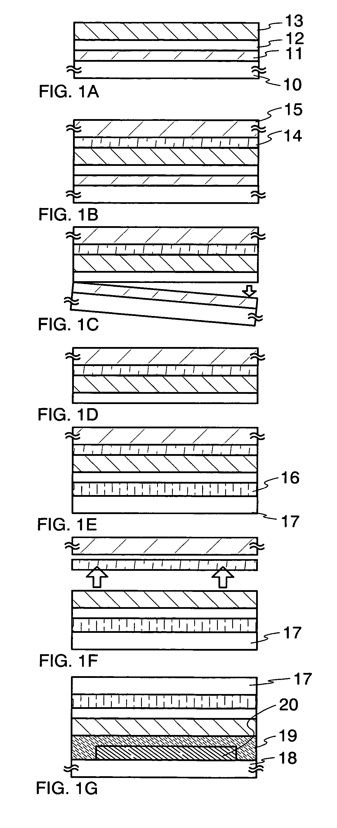
[0067]In Embodiment Mode 1, a peeling technique using a metal film and a silicon oxide film as disclosed in Japanese Patent Application Laid-Open No. 2003-174153 is employed. According to the peeling and transferring technique disclosed in Japanese Patent Application Laid-Open No. 2003-174153, a metal layer is formed over a substrate, and a metal oxide layer is formed in an interface between the metal layer and an oxide layer when laminating the oxide layer on the metal layer. By utilizing the metal oxide layer, peeling is performed in a subsequent step.
[0068]Concretely, a tungsten film is formed over a glass substrate by sputtering and then a silicon oxide film is laminated thereon by sputtering. When forming the silicon oxide film by sputtering, an amorphous tungsten oxide layer is formed. Elements such as a TFT are formed on the silicon oxide film. The substrate is subjected to a heat treatment of 400° C. or more in the element formation process such that the tungsten oxide layer...
embodiment mode 2
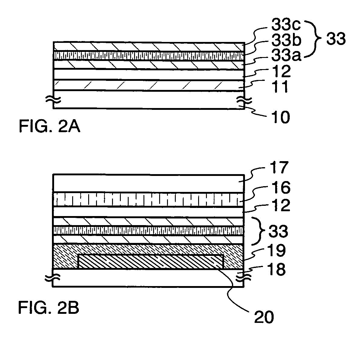
[0090]Differing from Embodiment Mode 1 that mainly explaining a single-layered protective film, Embodiment Mode 2 will show an example in which a protective lamination film including a stress relaxation film therein is peeled off and transferred with reference to FIGS. 2A and 2B. Note that, portions other than the protective lamination film are identical to those in Embodiment Mode 1, and will not be further explained. In FIGS. 2A and 2B, same portions as those in FIGS. 1A to 1G are denoted by same reference numerals.
[0091]The metal layer 11 and the oxide layer 12 are formed on the first substrate 10 in the same manner as Embodiment Mode 1. An inorganic insulating film, which becomes a first protective film 33a, is formed on the oxide layer 12 by PCVD. A planarized insulating film (a second protective film) is formed thereon as a stress relaxation layer 33b by application. An inorganic insulating film, which becomes a protective film 33c, is next formed on the stress relaxation laye...
embodiment mode 3
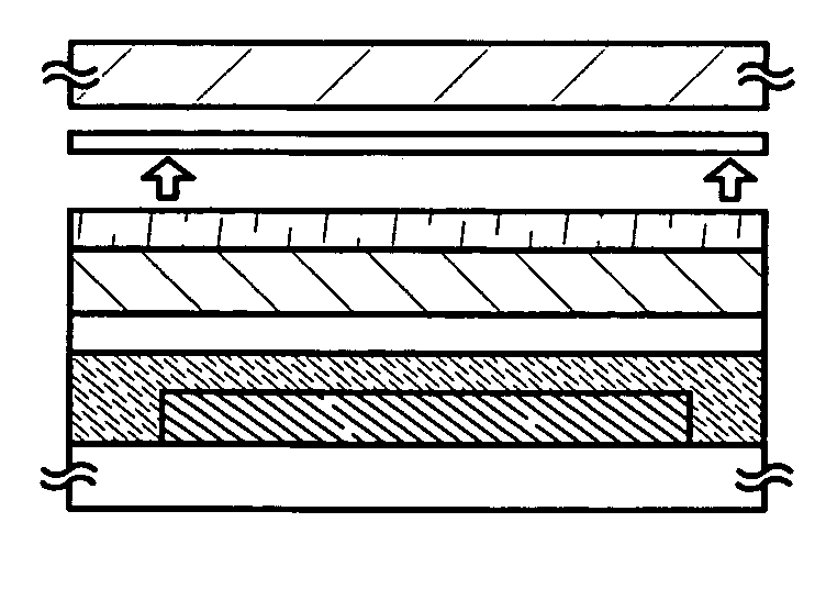
[0098]Differing from Embodiment Mode 1 showing an example in which a protective film is transferred over a film substrate and an element is sealed with the film substrate, Embodiment Mode 2 will show an example in which only a protective film is peeled off and transferred over a substrate with an element formed thereon to seal the element referring to FIGS. 3A to 3F. Note that, steps until forming the protective film are identical to those in Embodiment Mode 1, and will not be further explained. In FIGS. 3A to 3F, same portions as those in FIGS. 1A to 1G are denoted by same reference numerals.
[0099]The metal layer 11, the oxide layer 12, and the layer 13 to be peeled are sequentially formed on the first substrate 10 in the same manner as Embodiment Mode 1 (FIG. 3A, this figure shows a state after forming the layer to be peeled).
[0100]A protective layer made from an adhesive material that can be soluble in water or alcohols, that is, a water-soluble adhesive material 44 is applied on...
PUM
| Property | Measurement | Unit |
|---|---|---|
| temperatures | aaaaa | aaaaa |
| temperatures | aaaaa | aaaaa |
| transmittance | aaaaa | aaaaa |
Abstract
Description
Claims
Application Information