

Differential amplifier circuit capable of accurately amplifying even high-speeded signal of small amplitude
a technology of amplifier circuit and amplifier circuit, which is applied in the direction of pulse manipulation, pulse technique, instruments, etc., can solve the problems of slow signal transmission speed between main memory device such as dram and processor, and the inability to improve system performance further, so as to achieve accurate amplifying even a high-speed signal
- Summary
- Abstract
- Description
- Claims
- Application Information
AI Technical Summary
Benefits of technology
Problems solved by technology
Method used
Image

Examples
first embodiment
[0068]FIG. 8 is a circuit diagram showing a differential amplifier circuit according to the invention, which is a differential sense amplifier circuit of strong arm latch type including CMOS transistors.
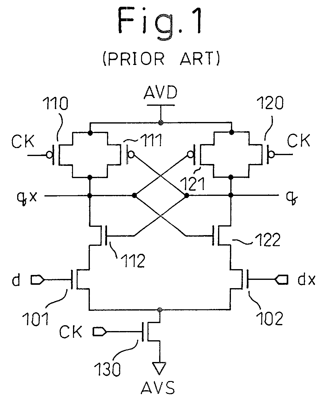
[0069]In FIG. 8, reference character AVD designates a high potential power line, character AVS a low potential power line, reference numerals 1, 2, 3, 12, 22, 30 N-channel MOS transistors (NMOS transistors), and numerals 10, 11, 20, 21 P-channel MOS transistors (PMOS transistors). Character CK designates a clock, characters d, dx differential input signals (complementary input signals) and characters q, qx differential output signals (complementary output signals, complementary output nodes). The transistors 11, 12 make up a first inverter, and the transistors 21, 22 make up a second inverter. The first and second inverters constitute a cross-coupled latch unit.
[0070]The source of the input transistor 1 having the gate thereof supplied with the input signal d and the source of the in...
second embodiment
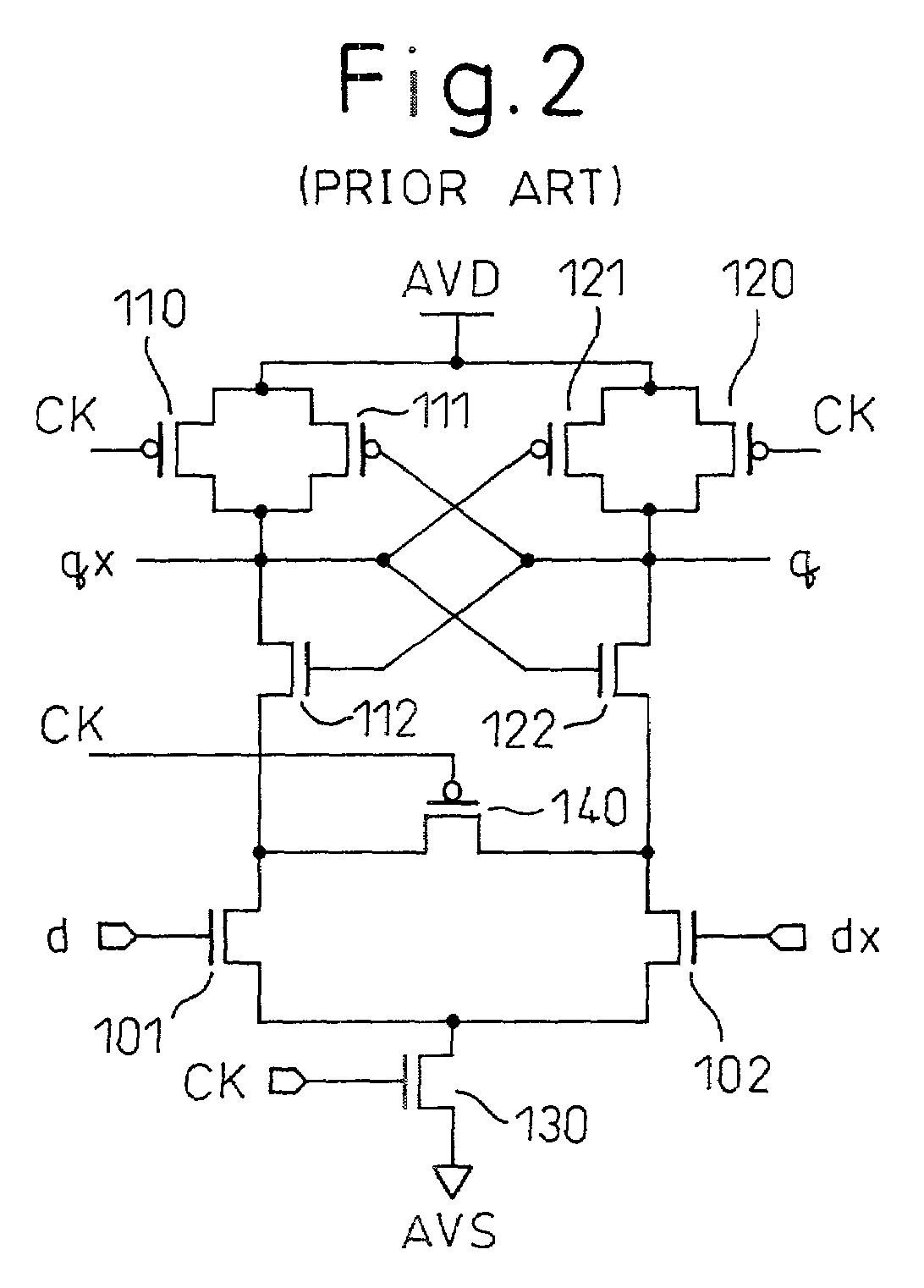
[0077] shown in FIG. 9, the drains of the transistors 1 and 2 are maintained at the same potential by the transistor 4 having the gate thereof supplied with the clock CK when the clock CK is at low level “L”, i.e. when the transistor 30 is off while the transistors 10 and 20 are on. As a result, the differential input transistors 1 and 2 are maintained at substantially the same potential when the signal is determined by changing the clock CK from low level “L” to high level “H”.
[0078]For signal determination, when the clock CK changes from low level “L” to high level “H”, the transistor 30 turns on and a current path is formed from the high potential power line AVD to the low potential power line AVS (ground GND) and the drive current flows. At the same time, the potential difference between the differential input signals d, dx causes the difference of the current flowing in the transistors 12 and 22. Therefore, the potentials of the nodes q, qx assume different values corresponding...
third embodiment
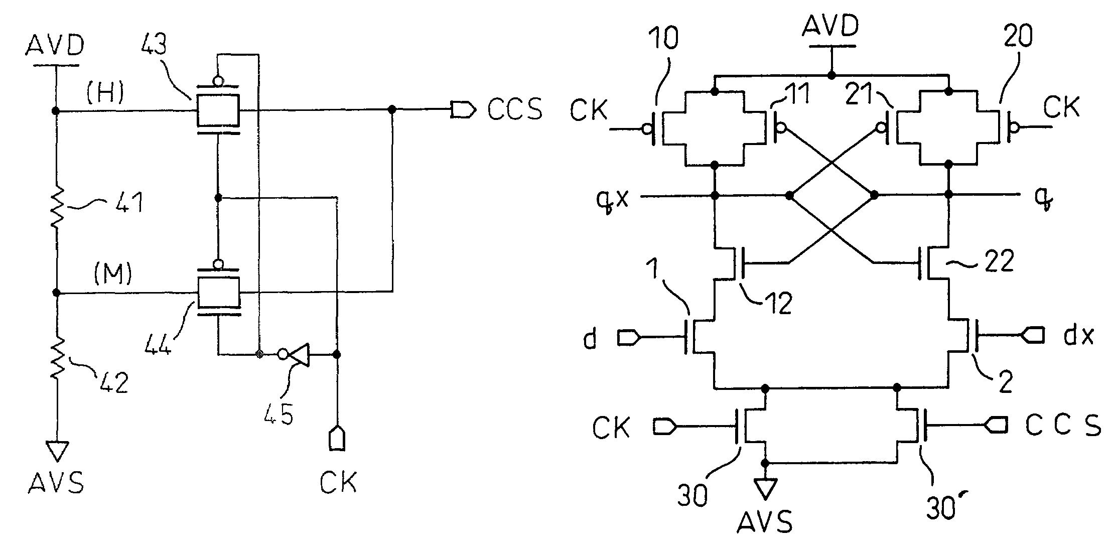
[0081]FIGS. 11A, 11B are diagrams showing a differential amplifier circuit according to the invention, in which FIG. 11A is a circuit diagram showing the differential amplifier circuit, and FIG. 11B a diagram showing a circuit for generating a current control signal.
[0082]As shown in FIG. 11A, the third embodiment corresponds to the differential amplifier circuit according to the first embodiment shown in FIG. 8, in which the transistor 30 doubles as the transistor 3. The circuit configuration of the third embodiment corresponds to that of the differential amplifier circuit of FIG. 1. In the third embodiment, however, the gate of the transistor 30′ is supplied with the current control signal CCS.
[0083]The current control signal CCS is generated by a circuit such as shown in FIG. 11B. In FIG. 11B, reference numerals 41, 42 designate resistor means, numerals 43, 44 transfer gates, and numeral 45 an inverter.
[0084]The input terminal of the transfer gate 43 is supplied with a high poten...
PUM
 Abstract
Description
Claims
Application Information